Direct current charging and discharging circuit, Electrical Engineering

Assignment Help:

1. The circuit shown below is a DC charging and discharging circuit.
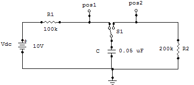
442_Find the time, t, in msec.png

a. At t = 0 sec, switch S1 is thrown to position 1 ("pos1"). Write the mathematical expressions for Vc (t) and Ic(t).

b. Find VC at t = 15 msec ("millisec") and at t = 30 msec.

c. Find IC at t = 0 msec and at t = 30 msec.

d. Find the time, t, in msec, that it will take for the capacitor to charge up to VC = 3 Volts.

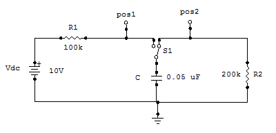
e. After t = 30 msec, the switch S1 is thrown into position 2 ("pos2"), as shown in the schematic below. Find VC when the switch is thrown to position 2, and find the current IC at the same instant.

f. Write the mathematical expressions for Vc (t) and Ic(t) for the time from the throwing of switch S1 to position 2 ("pos2").

g. Find VC at t = 20 msec after S1 goes to pos2.

h. Find VC and IC at t = 8 msec after S1 goes to pos2.

i.  How long does it take VC to fall to 3 Volts.
2166_Find the time, t, in msec 2.png


Related Discussions:- Direct current charging and discharging circuit

Game theory, an example and code for bargaining problem

an example and code for bargaining problem

Second Order Precesses, A second-order process with one pole at the origin ...

A second-order process with one pole at the origin has the transfer function 3/(s(2s + 1)) Find the output as a function of time, for a unit step input change. Sketch the expected

Explain common base configuration, Q. Explain common base configuration? ...

Q. Explain common base configuration? Common-base transistor amplifiers are so-called because the input and output voltage points share the base lead of the transistor in commo

Construction of a two stage rc coupled amplifier, Q. Describe the construct...

Q. Describe the construction of a two stage RC coupled amplifier with diagram. A cascaded arrangement of common-emitter transistor stages is shown above. The output Y1 of

Draw the circuit of a 7805 voltage regulator, Q. Draw the circuit of a 7805...

Q. Draw the circuit of a 7805 voltage regulator? Explain the functions of the capacitors used at its input and output sides. Functions of capacitors used at input and outp

Jump instruction - branch operations , Jump Instruction There are two ...

Jump Instruction There are two types of jump  instruction unconditional jump conditional jumps

Digital demodulator processes, Q. Digital demodulator processes? The fu...

Q. Digital demodulator processes? The functions of the receiver in Figure are the inverse of those in the transmitter. At the receiving end of a digital communication system, t

Realize the following boolean expression, Q. Using a minimum number of NAND...

Q. Using a minimum number of NAND gates, realize the following Boolean expression: F(A,B,C) = ∑ mi (0, 3, 4, 5, 7).

Explain noise, Explain Noise Noise is unwanted signals which degrade t...

Explain Noise Noise is unwanted signals which degrade the desired signal content and therefore the performance of the system. Noise might be produced either externally or inte

Bifurcation using simulink, i am implementing a paper "on the chaotic behav...

i am implementing a paper "on the chaotic behaviour of buck converter" a want to plot bifurcation diagram by using simulink blocks without using coding is it possible??

Write Your Message!

Captcha
Free Assignment Quote

Assured A++ Grade

Get guaranteed satisfaction & time on delivery in every assignment order you paid with us! We ensure premium quality solution document along with free turntin report!

All rights reserved! Copyrights ©2019-2020 ExpertsMind IT Educational Pvt Ltd