8279 Keyword /Display Controller :
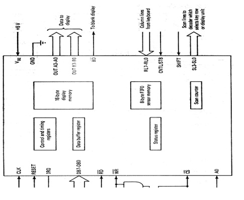
Figure shows the structure of 8279 and its interface to the bus. Addressing is according to the table given below.
CS RD WR AO Transfer Description
0 1 0 0 Data bus to data bus buffer
0 1 0 1 Data bus to control register
0 0 1 0 Data buffer register to data bus
0 0 1 1 Status register to data bus
8279 scans every row of the keyboard by sending out row addresses on SL2-SL0 and inputting signals on the return lines RL7-RL0, that are column addresses. When a depressed key is detected the key is automatically denounced by weighting 10 ms to check if the same key remains depressed. If a depressed key is detected and 8 bit code word corresponding to key position is assemble by joining column, shift and row position and control status as follows:
R-row (scan line address)
C-column (return line address)
The CNTL and SHFT pins are utilized to support control and shift keys. The key position is then entered into
8x8 FIFO sensor IRQ (Interrupt Request) and memory line are activated if sensor memory was previously empty.
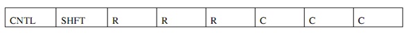
The timing and control registers are collection flags and registers that are accessed by commands. The 3 MSBs of the command decide its meaning and type of the remaining 5 bits. Out of 8 eight types of commands 3three commands are essential the formats of the three commands are as follows
Key board display mode set- it specifies the input and display methods and which is used in initialize the 8279. Its format is:
Control bits to set up input mode
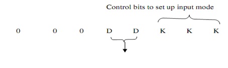
DD Control bits to set display modes
00-left entry, 8 8 bit displays
01- Left entry, 16 8 bit display
10-right entry, 8 8 bit displays
11-right entry, 16 8 bit displays
KKK
000 encoded keyboard scan mode having 2-key lockout
001 Decoded keyboard scan mode having 2 key lockouts.
010 encoded keyboard scan mode having N-key rollover
011 Decoded keyboard scan mode having N-key rollover
100 encoded sensor matrix scan mode
101 Decoder sensor matrix scan mode
110 strobe input having encoded display scan
111 strobe input having decoded display scan
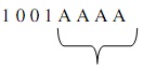
Read FIFO Sensor Memory:
It is denoted that a read operation from the data buffer register inputs a byte from the FIFO memory. In the sensor mode it particular which row has to be read. This command is required before inputting data from the FIFO memory. Its format is given below

Row address to be read in a sensor mode
Bit 4 is auto increment bit. If 1 next input is from the next byte in the FIFO Write to display memory:
Indicates that write to data buffer register will put data in display memory
Its format is
The address of the location in the display memory where the data for the next write will be stored 8279 provides 2 choice for handling the situation in which more than one key is depressed at approximate the same time. With the 2-key lockout choice, if another key is depressed whereas the first key is being denounced, the key which is released last will be entered into the FIFO. If the second key is depressed within 2 scan cycles after the first key is denounced and the first key remains depressed after the second one is released, then the first key is identified. If more than 1 is depressed, after they are depressed they all are entered in the order they were sensed.
8279 contain a sensor matrix mode in which signals in the return lines are stored into the FIFO at the row equivalent to the scan address.