Interrupt system based on 8259 a-microprocessor, Assembly Language

Assignment Help:

Interrupt System Based on Single 8259 A

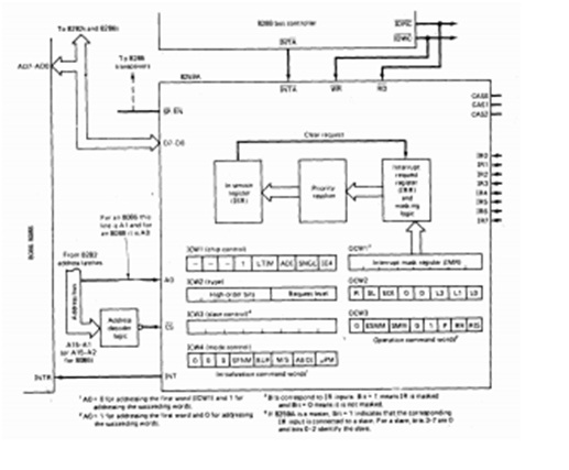
The 8259A is contained in a 28-pin dual-in-line package that need only a + 5-V supply voltage.  Its organization is shown in given figure along with its associates to a maximum mode system. Its pins (other than the ground pins and supply voltage) are defined as follows:

D7-DO - For communicating with the CPU over the data bus. On a few systems bus drivers might be required, but on the other systems direct connections can be used.

INT - It is used to send interrupt request signals to the CPU.

INTA - it is used to receive interrupt acknowledge signals from the CPU. The 8259A consider that an acknowledgment consists of two negative pulses, thus making it is compatible with 8086/8088 systems.

RD - it is used to signal the 8259A that it is to place the contents of the IRR ,ISR, or IMR, register or a priority level on the data bus. These possibilities is placed on the bus depends on the state of the 8259A and is discussed below.
1448_8259 A.jpg

WR - To signal the 8259A that it is to receive data from the data bus and us the data to set the bits in the command words.

CS - For indicating that the 8259A is being accessed. This pin is linked to the address bus through the decoder logic that compares the high-order bits of the address of the 8259A with the address presently on the address bus.  Input to this pin may be combined with S2 to give the ready signal.

AO - For indicating which port of the 8259A is being accessed.  2 addresses might be booked in the I/O address space for each 8259A in the system.

IR7-IRO - For receiving interrupt requests from I/O interfaces or other 8259As mentioned to as slaves.

CAS2-CASO - To recognize a specific slave device.

SP/EN  - For 1 of 2 purposes; either as an input to decide whether the 8259A is to be either as a slave (SP/EN = 0) or a master (SP/EN = 1) as an output to disable the data bus transceivers when data are being transferred from the 8259A to the CPU. Whether the SP/EN pin is utilized as an input or output depends on the buffer mode discussed below.


Related Discussions:- Interrupt system based on 8259 a-microprocessor

Selecting array elements, implement the following c++ code in assembly lang...

implement the following c++ code in assembly language using the block-structured .IF and .while directives

Icwi-microprocessor, The definitions of the bits in ICWI are following: ...

The definitions of the bits in ICWI are following: Always set to the value 1. It directs the received byte to ICWI as oppose to OCW2 or OCW3. Which also utilize the even addr

Display triangular shape using stars, write an assembly program to display ...

write an assembly program to display triangular star like shape

8086, to separate positive and negative numbers

to separate positive and negative numbers

Project, I need some guidance on which project to make in assembly language...

I need some guidance on which project to make in assembly language

Addressing modes for sequential control-microprocessor, The addressing mode...

The addressing modes for the sequential control transfer instructions are described below:   1. Immediate: Immediate data is a part of instruction,in this type of addressin

Dma hardware (8237 dmac)-microprocessor, DMA Hardware (8237 DMAC) : ...

DMA Hardware (8237 DMAC) :   1)Processor contain HOLD/HOLD Acknowledge lines to interact with 8237 o   DMAC can achieve control of ISA bus by asserting HOLD o   P

External hardware-interrupts-microprocessor, External Hardware-Interrupts ...

External Hardware-Interrupts External hardware-interrupts are generated by controllers of external devices or coprocessors and are connected to the processor pin for Non Mask a

Implemented with an arm assembly language program, The problem to be solved...

The problem to be solved and implemented with an ARM assembly language program You are asked to do some image processing on an image composed of characters shaped in For exa

Cache components-microprocessor, Cache components The cache sub-system ...

Cache components The cache sub-system may be divided into 3 functional blocks: Tag RAM, SRAM and theCache Controller. In real designs, these blocks can be implemented  by multi

Write Your Message!

Captcha
Free Assignment Quote

Assured A++ Grade

Get guaranteed satisfaction & time on delivery in every assignment order you paid with us! We ensure premium quality solution document along with free turntin report!

All rights reserved! Copyrights ©2019-2020 ExpertsMind IT Educational Pvt Ltd