Show quantization process, Electrical Engineering

Assignment Help:

Q. Show Quantization process

Let Figure (a) illustrate a message f (t) with values between 0 and 7 V. A sequence of exact samples taken at uniform intervals of time is shown: 1.60, 3.70, 4.75, 3.90, 3.45, and 5.85 V. Quantization consists of rounding exact sample values to the nearest of a set of discrete amplitudes called quantum levels. Assuming the quantizer to have eight quantum levels (0, 1, 2, . . . , 7 V), a sequence of quantized samples (2, 4, 5, 4, 3, and 6 V) is shown in Figure (a).

Obviously, the scheme is not limited to messages with only nonnegative voltages. The quantizer is said to be uniform when the step size between any two adjacent quantum levels is a constant, denoted by δv volts. Quantizers with nonuniform step size are also designed for improved system performance. An L-level quantizer can have even or odd L. A quantizer is said to be saturated or overloaded when

1969_Show Quantization process1.png

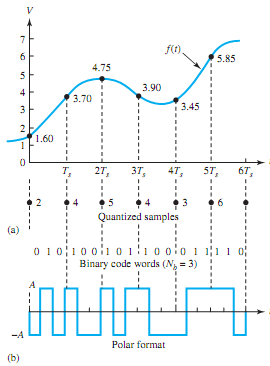
Figure shows the output quantum levels versus input voltage characteristic (stairstep in shape) of an L-level quantizer, when themessage signal has both positive and negative amplitudes of the same maximum magnitude. Case (a) corresponds to L being an even integer, when the midriser can be observed; and case (b) corresponds to L being an odd integer, when the midtread can be seen.


Related Discussions:- Show quantization process

Physics, what do we mean when we say that an equation is dimensionally corr...

what do we mean when we say that an equation is dimensionally correct?

Impedance heating system, Under what circumstances is individual circuit pr...

Under what circumstances is individual circuit protection for a lighting and applications panel board not required? What is the purpose of guarding runway contact conductors and

Show schematic arrangement of one- dimensional addressing, Q. Show the sche...

Q. Show the schematic arrangement for: (a) one- dimensional addressing, and (b) two-dimensional addressing, if a 32-kbit ROM is used to provide an 8-bit output word.

Lift interface circuitry, Draw the circuit diagram for  the  connections to...

Draw the circuit diagram for  the  connections to the EPROM and  just one RAM device  as defined  in  the memory map in question  3. You must show all the connections required to o

Evaluate the voltage gain, Q. On a CD amplifier R s = 4k?, µ =50 and r =35...

Q. On a CD amplifier R s = 4k?, µ =50 and r =35k?. Evaluate the voltage gain A v . A v = V o /V i = µRs / (µ+1)Rs + r

Single direction pump, Modify the design of the circuit shown in FIGURE and...

Modify the design of the circuit shown in FIGURE and draw a circuit diagram to provide rotary actuation in both directions using a single direction pump (to replace the bi-directio

Illustrate frequency-shift keying, Q. Illustrate Frequency-shift keying? ...

Q. Illustrate Frequency-shift keying? Digital transmission by FSK is a nonlinear modulation method that is appropriate for channels that lack the phase stability needed to perf

Explain low-frequency response of rc coupled amplifier, Q. Explain low-freq...

Q. Explain low-frequency response of RC coupled amplifier. What are the reasons for reduction in gain at low frequencies? The RC coupled amplifier circuit contains capacit

Write Your Message!

Captcha
Free Assignment Quote

Assured A++ Grade

Get guaranteed satisfaction & time on delivery in every assignment order you paid with us! We ensure premium quality solution document along with free turntin report!

All rights reserved! Copyrights ©2019-2020 ExpertsMind IT Educational Pvt Ltd