Phasor relation between different voltages and currents, Electrical Engineering

Assignment Help:

Phasor relation between different voltages and currents:

In the capacitive circuit of Figure, find

1.      Impedance,

2.      Resultant current,

3.      Power factor,

4.      Power absorbed by the circuit, and

5.      Phasor relation between different voltages and currents.
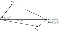
1317_Phasor relation between different voltages and currents.png

Figure

Solution

 (a)       The capacitive reactance is given by

                   X C =   1 / ωC  =     1/2π fC

=          1 / (2π× 50 × 1 × 10- 6)

= 3182.68 Ω

So the impedance, Z = R -j X C

                                     = 120 - j 3182.68 Ω

In polar form,  Z = 3184.94 ∠ - 87.84o Ω

(b)        Resultant current

          i =  v/ Z =  100 ∠ 0o / 3184.94 ∠- 87.84o

             = 0.03139 ∠ 87.84o Amp (leading)

(c)        Power factor, cos φ = cos 87.84o

                                                   = 0.0376 (lead)

 (d)       Power is absorbed only by resistor and that is also known as the active power in the circuit

P = I 2 R

= (0.03139)+ × 120

= 0.1182 Watts

 (e)       Voltage drop across resistor :

                          VR = iR

                                    = 0.03139 ∠ 87.84o × 120

                                       = 3.7668 ∠ 87.84o Volt (in phase with current i)

Voltage drop across capacitor

 Vc  = i (- j X c )

= 0.03139 ∠ 87.84 × 3182.68 ∠ - 90o

= 99.9 ∠ - 2.16o (lagging)

The phasor diagram is shown in Figure 4.25 and applied Voltage of 100 ∠ 0o is taken as reference.

2233_Phasor relation between different voltages and currents1.png

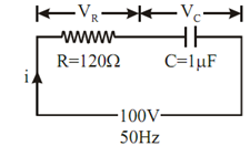
Figure: Phasor Diagram


Related Discussions:- Phasor relation between different voltages and currents

Zero flag - registers , Zero Flag - Registers If the  result of any  a...

Zero Flag - Registers If the  result of any  arithmetical  or logical  operation in the accumulator  is zero i ,e  all the bits  of accumulator  ( with  some exceptions )  are

DLD, DESIGN SR LATCH WITH UNIVARSAL LOGIC GATES.DRAW AND EXPLAIN THE LOGIC ...

DESIGN SR LATCH WITH UNIVARSAL LOGIC GATES.DRAW AND EXPLAIN THE LOGIC DIAGRAMS

Switching, With neat diagrams explain the configuration of a step-by-step s...

With neat diagrams explain the configuration of a step-by-step switching system

Fourier deconstruction, Find the Fourier series as far as the third harmoni...

Find the Fourier series as far as the third harmonic, to represent the periodic function y, given by the values in the following table. x 0 o 30

Explain integral-error or reset control, Q. Explain Integral-error or reset...

Q. Explain Integral-error or reset control? A control system is said to possess integral-error control when the generation of the output in some way depends upon the integral o

Evaluate the straight-line and actual gain response, Q. Consider the circui...

Q. Consider the circuit shown in Figure in the time domain aswell as in the s-domain. Its transfer function V 2 (s)/V 1 (s) can be shown to be  which is a second-order bandpass tra

Write Your Message!

Captcha
Free Assignment Quote

Assured A++ Grade

Get guaranteed satisfaction & time on delivery in every assignment order you paid with us! We ensure premium quality solution document along with free turntin report!

All rights reserved! Copyrights ©2019-2020 ExpertsMind IT Educational Pvt Ltd