Show operation on jfet, Electrical Engineering

Assignment Help:

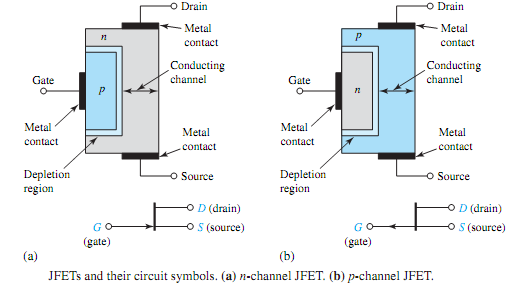
Q. Show Operation on JFET?

The junction in the JFETis reverse-biased for normal operation.No gate current flows because of the reverse bias and all carriers flow from source to drain. The corresponding drain current is dependent on the resistance of the channel and the drain-to-source voltage vDS.As vDS is increased for a given value of vGS, the junction is more heavily reverse-biased, when the depletion region extends further into the conducting channel. Increasing vDS will ultimately block or pinch off the conducting channel. After the pinch-off, the drain current iD will be constant, independent of vDS.

693_Show Operation on JFET1.png

It is the active region beyond pinch-off that is useful for the controlled-source operation, since only changes in vGS will produce changes in iD. Figure illustrates the JFET characteristics. Part (a) shows the idealized static characteristics with two regions separated by the dashed line, indicating the ohmic (controlled-resistance or triode) region and the active (controlled-source) region beyond pinch-off. Note that iD is initially proportional to vDS in the ohmic region where the JFET behaves much like a voltage-variable resistance; iD depends on vGS for a given value of vDS in the active region. In a practical JFET, however, the curves of iD versus vDS are not entirely flat in the active region but tend to increase slightly with vDS, as shown in Figure(b);

when extended, these curves tend to intersect at a point of -VA on the vDS axis. Another useful characteristic indicating the strength of the controlled source is the transfer characteristic, relating the drain current iD to the degree of the negative bias vGS applied between gate and source; a cutoff region exists, indicated by the pinch-off voltage -VP , for which no drain current flows, because both vGS and vDS act to eliminate the conducting channel completely.

Mathematically, the drain current in the active controlled-source region is approximately given by:

361_Show Operation on JFET.png

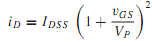
where IDSS, known as the drain-source saturation current, represents the value of iD when vGS = 0.


Related Discussions:- Show operation on jfet

Digital control system, block diagram of digital control system and explain...

block diagram of digital control system and explain each block

Explain mechanisms of propagation of radio communication, Explain mechanism...

Explain mechanisms of propagation of radio communication. Radio communication deals with electronic radiation of electromagnetic energy from one point to another through atmosp

Measurement, Why delay circuit used in CRO?

Why delay circuit used in CRO?

Elucidate the working of broad band ISDN, Q. Elucidate the working of broad...

Q. Elucidate the working of broad band ISDN? Ans: BISDN Configuration: Figuredemonstrates how access to BISDN network is accomplished. Every peripheral device is interfaced

Determine the capacitance length of a pcb embedded stripline, 1. Determine ...

1. Determine the capacitance length of a PCB embedded stripline, assuming no fringing of the electrostatic field. 2. Determine the capacitance/unit length of the same embedded stri

Convolution, how to use tabular method to solve convolution problems

how to use tabular method to solve convolution problems

Supernode, how does creating a supernode helps solve the problems?

how does creating a supernode helps solve the problems?

Explain node-voltage and mesh-current analyses, Explain Node-voltage and me...

Explain Node-voltage and mesh-current analyses? The node-voltage and mesh-current methods, which complement each other, are well-ordered systematic methods of analysis for solv

Explain the working of positive clamper, Q . Explain the working of Positiv...

Q . Explain the working of Positive Clamper? Positive Clamper: The circuit for a positive clamper is shown in the figure. During the negative half cycle of the input signal,

Calculate the power dissipated in the amplifier, For the amplifier circuit ...

For the amplifier circuit shown in Figure with R i ≅ ∞,R o ≅ 0,A = 10,R L = 100 , and v in = 1 V, calculate the power dissipated in the amplifier if the voltage at the power-s

Write Your Message!

Captcha
Free Assignment Quote

Assured A++ Grade

Get guaranteed satisfaction & time on delivery in every assignment order you paid with us! We ensure premium quality solution document along with free turntin report!

All rights reserved! Copyrights ©2019-2020 ExpertsMind IT Educational Pvt Ltd