Discuss electrical properties of insulating materials.
Electrical properties of an insulating material are As Follows:
Insulation resistance- It is the property, through the virtue of that, a material resists flow of electrical current. This must be high as possible. Two types of insulation resistance are:
(i) Volume resistance;
(ii) Surface resistance.
The resistance offered to the current, that flows by the material is termed as volume resistance. The resistance offered to the current, that flows over the surface of the insulating material is termed as surface resistance. Factors which affect the insulation resistance are as following-
a. Temperature variations
b. Exposure to moisture and
c. Voltage applied, aging.
Dielectric Strength- It is therefore the minimum voltage that when applied to an insulating material will effect in the destruction of its insulating properties. This can also be termed as the maximum potential gradient which the material can withstand without rupture, or without losing dielectric properties. The value is expressed in volts or kilovolts per unit thickness of insulating material. Such value is greatly affected through the conditions under that the material is operated. Factors, which affecting the dielectric strength are temperature and humidity.
Dielectric Constant- Every insulating material has got the fundamental property of storing charge (Q), while a voltage (V) is applied across this. The charge is proportional to the voltage applied that is Q α V, or Q = CV. Here C is termed as the capacity or capacitance of the material across that the voltage is applied. All insulating material behaves like a capacitor. Capacitance is differing for different insulating material. The property of insulating materials which causes difference in the value of capacitance, along with the physical dimensions remaining similar is termed as dielectric constant or permittivity (∈) and ∈ = C/Co, here C is capacity in presence of Dielectric and Co is the capacity in vacuum or air or in the absence of dielectric.
Dielectric loss and Loss angle: If a perfect insulation is subjected to alternating voltage, this is as applying alternate voltage to an ideal capacitor. Inside a perfect capacitor charging current would lead the applied voltage by 900 particularly. It means that there is no power loss in insulation. In mainly insulating materials it is not the case. Here is a definite amount of dissipation of energy when an insulator is subjected to alternating voltage. This dissipation of energy is termed as dielectric loss. Factors, which affecting dielectric loss are - Frequency of applied voltage, temperature and humidity increase and voltage.
The dielectric phase angle is θ and δ = 900 - θ is the dielectric loss angle as demonstrated in the figure below.
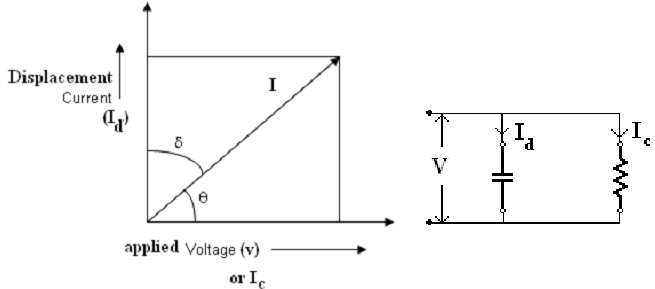
Also I is the phasor sum of Id and Ic , here Ic is the conduction current that is in phase along with the applied voltage and Id is the displacement current that is in quadrature phase along with applied voltage.