Dc charging and discharging circuit, Electrical Engineering

Assignment Help:

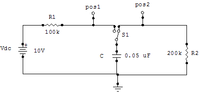
The circuit shown below is a DC charging and discharging circuit.

1743_DC charging and discharging circuit.png

a.  At t = 0 sec, switch S1 is thrown to position 1 ("pos1"). Write the mathematical expressions for and .

b.  Find VC at t = 15 msec ("millisec") and at t = 30 msec.

c.  Find IC at t = 0 msec and at t = 30 msec.

d.  Find the time, t, in msec, that it will take for the capacitor to charge up to VC = 3 Volts.

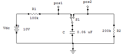
e.  After t = 30 msec, the switch S1 is thrown into position 2 ("pos2"), as shown in the schematic below. Find VC when the switch is thrown to position 2, and find the current IC at the same instant.

f.  Write the mathematical expressions for  and  for the time from the throwing of switch S1 to position 2 ("pos2").

g. Find VC at t = 20 msec after S1 goes to pos2.

h. Find VC and IC at t = 8 msec after S1 goes to pos2.

i. How long does it take VC to fall to 3 Volts.

1060_DC charging and discharging circuit1.png


Related Discussions:- Dc charging and discharging circuit

Regulation so significant, How does the ITU make sure compatibility among t...

How does the ITU make sure compatibility among the Radio systems used in dissimilar countries?  Why is regulation so significant?

Microcontroller interfacing, The winch uses a 415 Volt 50 Hz AC motor, so b...

The winch uses a 415 Volt 50 Hz AC motor, so both the up/down and run/stop controls actually operate +24V relays, whose contacts switch the 415Vac to the winch. The relays also pro

Show the dot convention, Q. For the coupled coils shown in Figure, a dot ha...

Q. For the coupled coils shown in Figure, a dot has been arbitrarily assigned to a terminal as indicated. Following the dot convention presented in the text, place the other dot in

Shocly equation, I need to prove of shockly diode equation

I need to prove of shockly diode equation

Phisics, deriving formula of the frictional force

deriving formula of the frictional force

Explain digital signal formatting, Q. Explain Digital Signal Formatting? ...

Q. Explain Digital Signal Formatting? After quantization and coding the samples of the message, a suitable waveform has to be chosen to represent the bits. This waveformcan the

Lift control unit, You are required to design and document  the hardware de...

You are required to design and document  the hardware design  for a 68HC12D60 based Lift Control Unit (LCU). This design includes  the Input/Output hardware for interfacing with  l

Mode 1 - buck converter , Mode 1 ( 0 By  applying a positive  output ...

Mode 1 ( 0 By  applying a positive  output  pulse  of the pulse  width modulator to  the  transistor Q 1 it gets turned on.  An input  current  in flows  through V in   Q 1

Calculus, area bounded by the curve y=3x(x-2)^2 and the x-axis

area bounded by the curve y=3x(x-2)^2 and the x-axis

Explain linear versus nonlinear control systems, Q. Explain Linear versus n...

Q. Explain Linear versus nonlinear control systems? Linear feedback control systems are idealized models that are conceived by the analyst for the sake of simplicity of analysi

Write Your Message!

Captcha
Free Assignment Quote

Assured A++ Grade

Get guaranteed satisfaction & time on delivery in every assignment order you paid with us! We ensure premium quality solution document along with free turntin report!

All rights reserved! Copyrights ©2019-2020 ExpertsMind IT Educational Pvt Ltd