Write a short note dispersion shifted dispersion flat fiber, Electrical Engineering

Assignment Help:

Write a short note on dispersion shifted and dispersion flatted fibers?

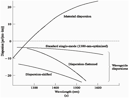
The dispersion features of a fiber is display below:
1090_flatted fibers.png

The overall dispersion is the sum of material dispersion and waveguide dispersion.
At wavelength larger than the zero material dispersion (ZMD) point within most general fibre designs, the material and waveguide elements are of opposite sign and can thus be made to cancel at a few longer wavelengths. Therefore the wavelength of first order chromatic dispersion can be shifted to the lowest loss wavelength for silicate glass fiber at 1.55 µm to gives both low dispersion and low loss fiber. This may be achieved through such mechanisms as a reduction in the fiber core diameter along with an accompanying raise in the relative or fractional index difference to create so known as dispersion shifted (DS) fiber.

An alternative modification of the dispersion characteristics of single mode fibers includes the achievement of a low dispersion window over the low loss wavelength region among 1.3 µm and 1.6 µm. like fibers, which relax the spectral requirements for optical sources and permit flexible wavelength division multiplexing are called as dispersion flatted (DF) fibers.

A huge variety of single mode fibers refractive index profiles are capable of modifications within order to tune the zero dispersion wavelength point λ0 to a exact wavelength inside a region adjacent to the zero material dispersion (ZMD) point. The simplest profile is in which of a step index fiber, as shown below:
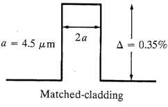
1021_matched cladding.png

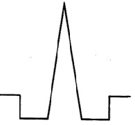
λ0 could be shifted to longer wavelength through altering the material composition of the fiber, which is through increasing the level of germanium doping in the fiber core. We use various profiles for DS as display below:
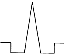
1084_Triangular profile.png

Fig: Triangular profile

1545_Depressed cladding triangular profile.png

Fig: Depressed cladding triangular profile
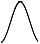
842_Gaussian profile.png

Fig: Gaussian profile

For better results we use advanced refractive index profiles like as
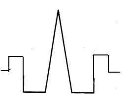
380_Triangular profile multiple index.png
Fig: Triangular profile multiple index
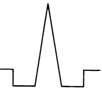
2477_segmented-core triangular profile design.png

Fig: segmented-core triangular profile design
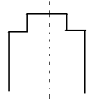
1159_Dual shaped core design.png

Fig: Dual shaped core design

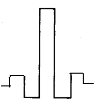
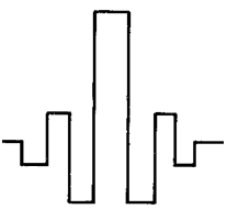
In dispersion flatted fibers there are two wavelengths of zero dispersion. For getting this window of low dispersion we use various profiles as display below:
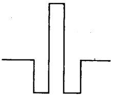
1299_Double clad.png

Fig: Double clad

112_Triple clad.png

Fig: Triple clad

740_quadruple clad.png

Fig: quadruple clad

The graphical representation of the DS and DF fibres is given below:
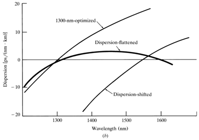
1109_DS and DF fibres.png


Related Discussions:- Write a short note dispersion shifted dispersion flat fiber

Military services - application of software defined radio, Military Service...

Military Services - Application of Software Defined Radio With the use of SDR technology, the military can reduce radio development costs by providing a common platform to whi

What is an amplifier, Q. What is an amplifier? What are the various types o...

Q. What is an amplifier? What are the various types of amplifiers? AMPLIFIER: A circuit that increases the amplitude of the given input signal is an amplifier. A small a.c. sig

Calculate the minimum sampling frequency, Three sine waves along with frequ...

Three sine waves along with frequencies 100Hz, 200Hz and 350Hz and with amplitudes of 1V, 2V and 1.5V correspondingly, are added together to make a single waveform. What is the min

Distribution transformers, Distribution Transformers 1. Augmentation/...

Distribution Transformers 1. Augmentation/Addition of Distribution Transformers Distribution transformers have to be augmented by installing additional transformers or in

Calulation of hv/lv ratio to reduce the line loss, kindly send us the formu...

kindly send us the formula and C program for performance improvement of distribution system using HV/LV ratio. REGARDS ANUJ AGARWALA

Minimized circuit not -or and gate, 1.  Given S(D1) = !Q1 X + !Q1 Q0 + Q1 !...

1.  Given S(D1) = !Q1 X + !Q1 Q0 + Q1 !Q0 !X                                                        and       S(D0) = !Q1 !Q0 !X + Q0 X + Q1 !Q0 !X       A.  DRAW A MINIMI

Logic Gates, XOR gate BY using NAND gate Only

XOR gate BY using NAND gate Only

Wireless and communication, With a maximum excess delay of and a chip durat...

With a maximum excess delay of and a chip duration of , the multipath components fall in delay bins. This means that we experience leakage of energy between chips and the channel i

Why biasing in necessary in transistor, (a) Describe why ordinary junction ...

(a) Describe why ordinary junction transistor is known as bipolar. (b) Describe working of NPN transistor as common Base configuration. Describe working of NPN transistor in

Capacitive var, how over compensation by capacitive var rises voltage in a ...

how over compensation by capacitive var rises voltage in a circuit?

Write Your Message!

Captcha
Free Assignment Quote

Assured A++ Grade

Get guaranteed satisfaction & time on delivery in every assignment order you paid with us! We ensure premium quality solution document along with free turntin report!

All rights reserved! Copyrights ©2019-2020 ExpertsMind IT Educational Pvt Ltd