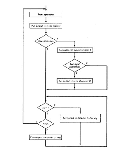
Flowchart for the sequence of 8251
Whether the control, mode or sync character register is selected depends on the accessing sequence. A flowchart of the sequencing is given in the given figure. After a hardware reset or a command is given with its reset bit set to one, the next output with A0 value 1(for example, with C/D=1,WR=1, and CD=0) is directed to the mode register. The formats of the mode register for the asynchronous and synchronous both cases are defined in given figure. If the 2 LSBs of the mode are 0, then the interface is put in its synchronous mode and the MSB determines the number of sync characters. In the synchronous mode, the next one or two bytes output with A0 value 1 become the sync characters. If the 2 LSBs of the mode are not both zero, then the 8251A enters its asynchronous mode. In other case, all subsequent bytes prior to another reset go to the control register if A0 value is 1 and the data-out buffer register if A0 value is 0.
In the synchronous mode the baud rates of the receiver and transmitter , which are the shift rates of the shift registers, are the similar as the frequencies of the signals applied to RxC and TxC, respectively, but in the asynchronous mode the 3 remaining possible combinations for the 2 LSBs in the mode register dictate the baud rate factor. The relationship amongst the frequencies of the RxC and TxC clock inputs and the baud rates of the transmitter and receiver is:
Clock frequency is equal to Baud rate factor x Baud rate.
If 10 is in the LSBs of the mode register and the receiver and transmitter baud rates are to be 1200 and 300, respectively, then the frequency applied to TxC would be 4800 Hz and the frequency at RxC should be 19.2 kHz. In the asynchronous and synchronous both modes, bits two and three denote the number of data bits in each character, bit four denote whether or not there is to be parity bit, and bit five indicate the type of parity (even or odd). For the asynchronous mode the 2 MSBs denote the number of stop bits, but for the synchronous mode bit six determines whether the SYNDET pin is to be utilized as an input or as an output and, as mentioned above, bit seven indicates the number of sync characters.
If the SYNDET pin is utilized as an output it becomes active when a bit-for-bit match has been found between the sync character(s) and incoming bit stream. If the search for sync characters is conducted by an external device, then SYNDET may be used to input a signal, denoting that a match has been found by the external device. Also the pin has a meaning during asynchronous operation, but in this case it may just be an output. This output is known the break detect signal and goes high whenever a character consisting of all 0s is received.