With the help of a neat diagram, explain the working of a successive approximation A/D converter
Ans:
Successive Approximation ADC:
It is the most broadly used A/D converter. By the name suggests, the digital output tends towards analog input by successive approximations. While Successive Approximation ADC, the comparison along with the input analog voltage is completed in descending order starting from the maximum voltage. Fig.(a) demonstrates the block diagram of SA A/D converter. The major elements are Op-amp Comparator, SA register, Control Logic and D/A converter. This uses Digital to Analog converter like a feedback component. The control logic is the most significant part of Successive Approximation Converter, as it decides the next step to be occupied. The ring counter gives timing waveform to control the operation of the converter. The Digital to Analog Converter unit, n bit register and ring counter are all reset through the first pulse from the ring counter. The ring counter having a single one sets the MSB of the Digital to Analog Converter for 1 and another to 0.
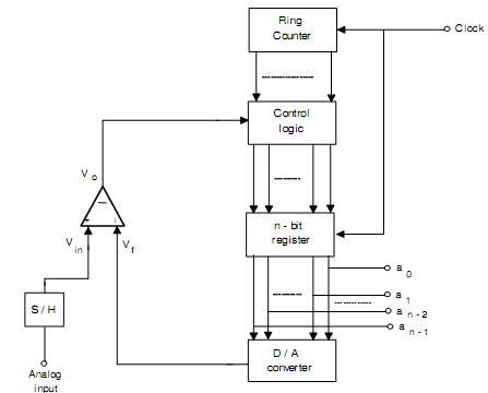
Fig.(a) Block Diagram of Successive Approximation A/D Converter
The fundamental operating principle of Successive Approximation A/D Converter is that the voltage output of DAC consequent to MSB is compared through the comparator along with the input voltage and the bit 1 is retained, if the voltage is less. If the voltage is more, this is reset to 0 and counter moves to subsequent position. The same decisions are made at each bit position till the nearest value is reached.
Suppose that the MSB of a unipolar 6 bit converter generates 10 V output and we should measure an analog output voltage of 8.2 V. All bits divide the voltage with 2 therefore the voltages for the 6 bits from MSB downwards are:
Bits 5 4 3 2 1 0
Voltage 10 5 2.5 1.25 0.625 0.3125
MSB LSB
The operation of SA A/D converter is illustrated in Table no.(a). Assume that the analog input be 8.2 V. The SA register is firstly set to zero. After that 10 is placed in MSB. It is fed to D/A converter whose output goes to comparator. Because the analog input (8.2 V) is greater than D to A output (that is, 10 V), the MSB is set to one. After that 1 is placed in bit next to MSB (that is, 1 is placed in second position). At this time the output of D/A is 5 V. Because analog input is less than 5 V, this is reset to 0. Next 0 is placed in third position. Now the D/A output is (5+2.5=7.5V) which is less than analog input. Thus, this 0 bit is retained and 0 is positioned in the next bit (that is, fourth position). This time the D/A output is (7.5+1.25=8.75), that is more than analog input. Thus, the 1 bit is placed in fifth position. At this moment the D/A output is (8.75+0.625=8.125) that is less than analog input, this is reset to 0. Currently 0 is placed in LSB producing a D/A output of (8.125+0.3125=8.4375) that is more than analog input. Thus, LSB is set to one.
The different steps and voltages are tabulated in Table no. (a).
|
Step
|
Register
|
DAC OutputComparator decision
|
Comparator decision
w.r.t 8.2V.
|
|
Start
2
3
4
5
6
|
100000
010000
011000
011100
011010
011011
|
10
5
5+2.5=7.5
7.5+1.25=8.75
7.5+0.625=8.125
8.125+0.3125=8.4375
|
High
Low
Low
High
Low
High
|
Table (a)
The D/A converter waveform is demonstrated in fig. (b)
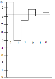
Fig.(b) Output Waveform of D/A Converter
Features:
(i) This is one of the most widely used ADC
(ii) Conversion time of this is very next simply to Flash or Parallel ADC
(iii) SACs contain fixed value of conversion time which is not dependent upon the value of analog input voltage.
(iv) Data can be taken out either in parallel or in serial.
(v) Throughout the period of comparison the input analog voltage must be held constant and therefore the input to comparator is by a Sample Hold circuit.