With the help of clocked JK flip flops and waveforms, explain the working of a three bit binary ripple counter. Write truth table for clock transitions.
Ans. Three-Bit Binary Ripple Counter: Into Ripple Counters, each Flip-flop are not clocked concurrently and the flip-flops do not change state accurately at the similar time. A three-bit Binary Counter has maximum of 23 states that is, 8 states, that needs 3 Flip-Flops. The word Binary Counter implies a counter that counts and makes binary outputs 000,001,010--111. This goes through a binary sequence of 8 different states (that is from 0 to 7). Fig.(a) demonstrates the logic circuit of a three-bit Binary Ripple Counter having 3 Edge Triggered JK flip-flops. Here indicated by tiny circles at the CLK input of flip- flops, the triggering happens while CLK input finds a negative edge. Q0 is the Least Significant Bit i.e. LSB and Q2 is the Most Significant Bit i.e. MSB. The flip-flops are linked in series. The Q0 output is linked to CLK terminal of second flip-flop. The Q1 output is linked to CLK terminal of 3rd flip-flop. This is termed as a Ripple Counter since the carry moves by the flip-flops like a ripple on water.
Working: Initially, CLR is changed to Low and all flip-flops Reset providing an output Q = 000. While CLR becomes High, the counter is get ready to start. As LSB gets its clock pulse, the total output Q = 001 and its output changes from 0 to 1. While second clock pulse arrives, Q0 resets and carries (that is, Q0 goes from 1 to 0 and, second flip flop will receive CLK input. There is the output is Q = 010. The third CLK pulse changing from Q0 to 1 providing a total output Q = 011. The fourth CLK pulse because of Q0 to reset and carry and Q1 also resets and carries providing a total output Q = 100 and thus the process goes on. The action is illustrated is Table. The no. of output states of a counter is termed as Modulus or Mod. A Ripple Counter along with 3 flip-flops can count 0 to 7 and is thus, termed as Mod-8 counter.
| Counter State |
Q2
|
Q1
|
Q0
|
|
0
|
0
|
0
|
0
|
|
1
|
0
|
0
|
1
|
|
2
|
0
|
1
|
0
|
|
3
|
0
|
1
|
1
|
|
4
|
1
|
0
|
0
|
|
5
|
1
|
0
|
1
|
|
6
|
1
|
1
|
0
|
|
7
|
1
|
1
|
1
|
Table: Counting Sequence of a 3-bit Binary Ripple Counter
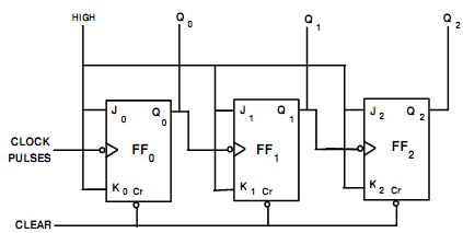
Fig.(a) Logic Diagram of 3-Bit Binary Ripple Counter
Ripple counters are easy to fabricate but contain the problem as the carry has to propagate by a no. of flip flops. The delay times of whole the flip flops are added. Thus, they are extremely slow for several applications. The other problem is that unnecessary pulses happen at the output of gates.
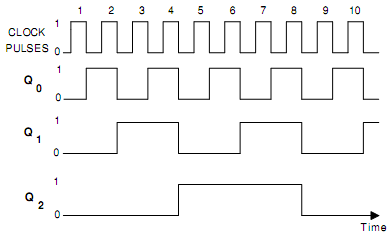
Fig.(b) Timing Diagram of 3-bit Binary Ripple Counter
The timing diagram is demonstrated in Fig.(b). Here FF0 is LSB flip flop as well as FF2 is the MSB flip flop. Because FF0 obtains each clock pulse, Q0 toggles once per negative clock edge as demonstrated in Fig. (b). All remaining flip flops toggle less frequently since they receive negative clock edge through preceding flip flops. While Q0 goes from 1 to 0, FF1 obtains a negative edge and toggles. Likewise, when Q1 changes 1 to 0, FF2 obtains a negative edge and toggles. At last when Q2 changes 1 to 0, FF3 obtains a negative edge and toggles. Therefore, whenever a flip flop resets to 0, the subsequent higher flip flop toggles.
This counter is termed as ripple counter since the 8th clock pulse is applied; the trailing edges of 8th pulse cause a transition in every flip flop. So Q0 goes from High to Low, it causes Q1 go from High to Low that causes Q2 to go from High to Low that causes Q3 to go from High to Low. Therefore the effect ripples throughout the counter. This is the delay caused by this ripple that results in a limitation upon the maximum frequency of input signal.