Explain a TTL NAND gate and its operation, Computer Engineering

Assignment Help:

Give the circuit of a TTL NAND gate and explain its operation in brief.

Ans:

Operation of TTL NAND Gate: Fig.(d) Demonstrates a TTL NAND gate with a totem pole output.   The    totem pole output implies that transistor T4 sits atop T3 in order to give low output impedance.  The low output impedance means a short time constant RC therefore the output can change rapidly from one state to the other. T1 is a multiple type emitter transistor. Such transistor can be thought of like a combination of various transistors along with a common collector and base. Multiple emitter transistors along with about 60 emitters have been developed. In this figure, T1 has 3 emitters thus there can be three inputs A, B, C. The transistor T2 functions as a phase splitter since the emitter voltage is out of phase along with the collector voltage. The transistors T3 and T4 by the totem pole output, the capacitance CL shows the stray capacitance and so on. The diode D is added to make sure that T4 is cut off while output is low. The voltage drop of diode D remains the base-emitter junction of T4 reverse biased therefore only T3 conducts while output is low. The operation can be described briefly by three conditions as specified below:

Condition 1: At least one input is low (that is, 0).  Transistor T1 saturates. Thus, the base voltage of T2 is almost zero. T2 is cut off and forces T3 to cut off.  T4 functions as an emitter follower and couples a high voltage to load. Output is high (that is Y=1).

Condition 2: Each input is high. The emitter base junctions of T1 are reverse biased. The collector base junction of T1 is forward biased. Therefore, T1 is in reverse active mode. The collector current of T1 flows in reverse direction. Because this current is flowing in the base of T2, the transistors T2 and T3 saturate and then output Y is low.

Condition 3: The circuit is operating under II while one of the inputs becomes low. The consequent emitter base junction of T1 starts conducting and T1 base voltage drops to a low value.  Thus, T1 is in forward active mode. The high collector current of T1 shifts the stored charge in T2 and T3 and hence, T2 and T3 go to cut-off and T1 saturates and then output Y returns to high.

1437_Logic Diagram of TTL NAND Gate with Totem Pole Output.png

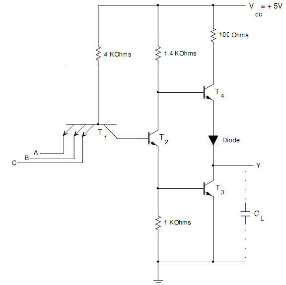
Fig.(d) Logic Diagram of TTL NAND Gate with Totem Pole Output


Related Discussions:- Explain a TTL NAND gate and its operation

What is common control switching system, What is common control switching s...

What is common control switching system? Explain. Common Control Switching System: It is a functional block diagram of a common control switching system is demonstrated in figu

Derive the expression of traffic capacity, Traffic Capacity is given by? ...

Traffic Capacity is given by? Traffic Capacity = Switching capacity × Theoretical maximum load.

Explain about flip-flops, Explain about Flip-Flops  Flip-Flops are also...

Explain about Flip-Flops  Flip-Flops are also called bistable multivibrator.  A flip-flop is capable of storing 1 bit of binary data.  It has two stable states- 'one' and 'zero

New execution of listpermutations, Update the permutation algorithm from th...

Update the permutation algorithm from the text to obtainthe correct list of permutations even if the string haves repeated letters. For example, if you call ListPermutations on the

What is visualisation - search based tools, Q. What is Visualisation - sear...

Q. What is Visualisation - search based tools? Visualization is a common method in contract to search based tools. In this scheme visual aids are supplied as pictures to help p

Explain what are the different hazards, There are situations, called hazard...

There are situations, called hazards that stop the next instruction in the instruction stream from implementing during its designated clock cycle. Hazards decrease the performance

Using the editor or debugger, Write a script that will read from a file x a...

Write a script that will read from a file x and y data points in the following format: x   0    y  1 x  1.3  y  2.2 x  2.2  y  6 x  3.4  y  7.4 The format of each line in the

What is stack pointer, Stack pointer is a particular purpose 16-bit registe...

Stack pointer is a particular purpose 16-bit register in the Microprocessor, which grasp the address of the top of the stack.

Programming, Which is the best programming language to learn?

Which is the best programming language to learn?

How to correctly apply the graphics patches in matlab, Open a LOCAL MACHINE...

Open a LOCAL MACHINE window and type: xhost +ashland # Add the following code sequence just before the plot command that was giving you problems: figure; set(gcf,'renderer','zbuffe

Write Your Message!

Captcha
Free Assignment Quote

Assured A++ Grade

Get guaranteed satisfaction & time on delivery in every assignment order you paid with us! We ensure premium quality solution document along with free turntin report!

All rights reserved! Copyrights ©2019-2020 ExpertsMind IT Educational Pvt Ltd