Q. Sketch An Rc Coupled Two Stage Amplifier. Draw Its Frequency Response Curve And Account For Its Stages.
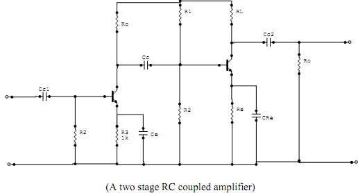
The figure above shows a two stage RC coupled amplifier. The signal developed across collector resistor Rc of the first stage is coupled with the base of the second stage through a capacitor Cc. The coupling capacitor Cc blocks DC voltage from first stage, from reaching the second stage. So the DC biasing of the next stage is not interfered with. Hence Cc is also known as blocking capacitances.
Some loss of signal voltage always occurs due to drop across Cc. If we are amplifying signals above 10 hz, the scheme is more suitable. It is a convenient and least expensive way of building a multistage amplifier.
RC coupled amplifier finds its application in amplifiers used in TV,radio,tape recorders etc.
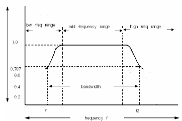
FREQUENCY RESPONSE CURVE:
The performance of an amplifier is judged by observing whether all frequency components are amplified equally well. This we can observe on the frequency response curve.The curve illustrates how the magnitude of voltage gain of an amplifier varies with the frequency of the input signal.It can be plotted by measuring the voltage gain for different frequencies of the sinusoidal voltage fed to the input. The gain is constant for a limited band of frequencies.This frequency is called mid frequency range and mid band gain Avm.
On both sides of mid gain, the gain decreases.In mid frequency range,the coupling capacitor and the bypass capacitor works as good as being short circuited.
But when frequenc is low,the capacitors have greater value of reactance, since the reactance of the capacitor Xc= 1/2?fC.
The coupling capacitor affects the gain of the amplifier at low frequencies. R1 and R2 are the biasing resistors. Assuming that the bypasss capacitor is replaced by a short circuit.R1 and R2 are the input impedance of the next stage,which are in parallel and equivalent to the resistance R. The coupling capacitor Cc is in series with R and this series combination is in parallel with the collector resistor Rc.The whole of this impedance forms the AC load for the preceding stage. But the effective output of this stage, is the AC voltage developed across the resistor R. At the mid frequency the reactance of Cc is sufficiently small compared to the R.
We can treat it as a short circuit. R comes in parallel with Re. in which case the voltage across Rc will be the same as the voltage across R.But at low frequencies, the reactance of Cc, is sufficiently large causing significant drop across Cc. As a result, the output voltage decreases.Lower the frequency of the signal higher will be the reactance of Cc, and more will be the reduction in output voltage.
Lower the frequency , higher will be the impedance of Ce, and greater is the reduction in gain. Due to the coupling capacitor Cc, the effective output voltage is reduced at low frequency, which is also responsible for the decrease of gain at low frequencies.
In mid frequency range(50 Hz to 20KHz),the voltage gain of the amplifier is constant, as is from the analysis. With the increase in the frequency in this range, the reactance of the coupling capacitor Cc reduces thereby increasing the gain but at the same time lowercapacitive reactance causes higher loading resulting in lower voltage gain. Thus the two effects cancel each other and uniform gain is obtained in mid frequency range. At low frequency range(below 50 Hz), higher capacitive reactance of coupling capacitor Cc allows very small part of signal to pass from one stage to the next and also because of higher reactance of emitter bypass capacitor CE, allows very small part of signal to pass from one stage to the next and also because of higher reactance of emitter bypass capacitor CE, the emitter resistor RE is not effectively shunted. Thus the voltage gain falls off at low frequencies.