Design a MOD-6 synchronous counter using J-K Flip-Flops.
Ans:
Design of Mod-6 Counter: To design the Mod-6 synchronous counter, contain six counter states (that is, from 0 to 6). For this counter, the counter design table lists the three flip-flop and their states as 0 to 6 and the 6 inputs for the 3 flip-flops. The flip-flop inputs essential to step up the counter from the now to the next state is worked out along with the help of the excitation table. The needed counter states and the J K inputs essential for counter flip- flops are specified in the counter design table demonstrated in Table no.1.
|
Input pulse
count
|
Counter States
|
|
Flip-Flop Inputs
|
|
A B C
|
JA
|
KA
|
JB KB
|
JC KC
|
|
0
|
0 0 0
|
1 X
|
0 X
|
0 X
|
|
1
|
1 0 0
|
X 1
|
1 X
|
0 X
|
|
2
|
0 1 0
|
1 X
|
X 0
|
0 X
|
|
3
|
1 1 0
|
X 1
|
X 1
|
1 X
|
|
4
|
0 0 1
|
1 X
|
0 X
|
X 0
|
|
5
|
1 0 1
|
X 1
|
0 X
|
X 1
|
|
6(0)
|
0 0 0
|
|
|
|
Table no.1: Counters Design Table for Mod-6 Counter
Flip-Flop A:
The primary state is 0. This change to 1 after the clock pulses. Thus, JA must be 1 and KA may be 0 or 1 (that is X). In the subsequent state 1 change to 0 after the clock pulse. Hence, JA may be 0 or 1 (that is, X) and KA must be 1.
Flip-Flop B:
The primary state is 0 and this remains unchanged after the clock pulse. Hence, JB must be 0 and KB may be 0 or 1 (i.e. X). In the subsequent state 0 changes to 1 after the clock pulse. Hence, JB must be 1 and KB may be 0 or 1 (that is, X).
Flip-Flop C:
The primary state is 0 and this remains unchanged after the clock pulse. Hence JC must be 0 and KC may be 0 or 1 (that is, X). In the subsequent state, this remains unchanged after the clock pulse. Thus, JC must be 0 and KC may be 0 or 1 (that is, X).The JK inputs needed for such have been found with the help of the excitation table, (as in table no.1). The flip-flop input values are entered into Karnaugh maps demonstrated in Fig. a [(i), (ii), (iii), (iv), (v) and (vi)] and a Boolean expression is determined for the inputs to the three flip-flops and then all expressions are simplified. As all the counter states have not been utilized, Xs (don't) are entered to denote un-utilized states. The expressions that simplified for each input have been demonstrated under each map. At last, these minimal expressions for the flip-flop inputs are utilized to draw a logic diagram for the counter demonstrated in fig.(b).
As before, the JK inputs needed for this have been found with the help of the excitation table, (as in table no.1). Such input values are entered in Karnaugh maps Fig. (a)[i to vi] and a Boolean expression is determined for the inputs to the three flip-flops and then all expressions are simplified. Xs have been entered in that counter states that have not been utilized. The simplified expressions for all inputs have been demonstrated under each map and at last a logic diagram based upon these expressions is drawn and is demonstrated in fig.(b).
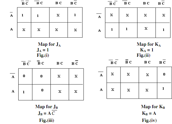
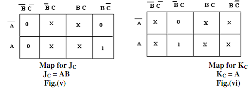
Fig.(b) Karnaugh Maps for JA,KA,JB,KB,JC,KC
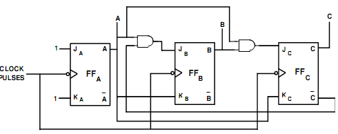
Fig.(c) Logic Diagram for MOD-6 Synchronous Counter