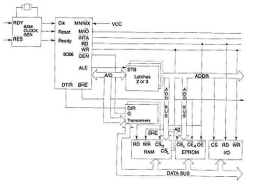
8086 Minimum mode System and Timing
In a minimum mode 8086 system, the microprocessor 8086 is operated in minimum mode by strapping its MN/MX pin to logic 1.All the control signals in this mode are given by the microprocessor chip itself. In the minimum mode system there is singlemicroprocessor.In the systemthe remaining components are Trans receivers, I/Odevise, latches clock generator andmemory. Some type of chip selection logic may be required for selecting memory or I/O devices, depending upon the address map of the system.
In General the latches are buffered output D-type flip-flops, like74LS373 or8282 They are used for separating the valid address from the multiplexed address/data signals and are controlled by the ALE signal generated by 8086. Tran receivers are the bi-directional buffers and sometimes they are calledas data amplifiers. They are required to choose the valid data from the time multiplexed address/data signal. They are controlled by two signals that name areDT/R and DEN. The DEN signal indicates that the valid data is available on the data bus, when DT/R denoted the direction of data, for example from or to the processor. The system consist memory for the users and monitorprogram storage. generally EPROMS are utilized for monitor storage, when RAMs for users program storage. A system can contain I/O devices for communication with the processor as well as some special purpose I/O devices. The clock generator generates the clock from the crystal oscillator and then shapes it and divides to make it more precise so that it may be used as an accurate timing reference for the system. The clock generator synchronizes some external signals also with the system clock. The common system organization is shown in given figure Since it has twenty address lines and sixteen data lines, the 8086 CPU requires 3 octal address latches and 2 octal data buffers for the complete address and data separation.
The working of the minimum mode configuration system may be better described in terms of the timing diagrams rather than qualitatively describing the operations. The opcode fetch and read cycles are same. So the timing diagram may be categorized in 2 parts) the first is the timing diagram for read cycle and the second is the timing diagram for write cycle.
The read cycle start in T1 with the assertion of the address latch enable (ALE) signal and also M/IO signal. During the -ve going edge of this signal, the valid address is latched upon the local bus. The A0and BHE signals address high,low or both bytes. From T1 to T4, the IO and memory signal indicates a memory or I/O operation. At T2, the address isremoved from the local bus and is sent to the output. The bus is then tristated. Also the read (RD) control signal is activated in T2. The read (RD) signal causes the addressed device to enable its data bus drivers. After RD goes low, the valid data is available on the data bus. The addressed device will make the READY line high. When the processor returns the read signal to high level, the addressed device will tristate its bus driversagain.
A write cycle also starts with the assertion of ALE and the emission of the address. The M/IO signal is again asserted to denotean I/O or memory operation.After sending the address in T2, InTg, the processor sends the data to be written to the addressed location. The data remains on the bus till middle of T4 state. The WR becomes active at the starting of T2 (unlike RD is somewhat delayed in T2 to provide time for floating).
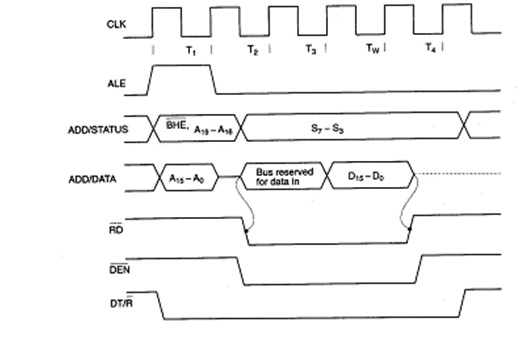
Figure : Read cyde Timing Diagram for Minimum Mode