Reference no: EM132549815
ELEC 20008 Microprocessors and Interfacing - Middel East College
Learning Outcome 1: Use various programming techniques to program 8085 microprocessor;
Learning Outcome 2: Describe single and multiple interrupts;
Learning Outcome 3: Interface memory and I/O devices to microprocessor.
Assignment Objective
Assignment will enable each student to get an insight about various programming techniques of 8085 microprocessor. In addition to this, some topics about interrupts and interfacing concepts will develop student's critical thinking, logical reasoning, programming and problem solving skills related to microprocessor systems.
Assignment Tasks:
For the memory interface shown in figure 1, determine the memory map.
Figure 1
For the memory interface shownin figure 2, determine the memory map.
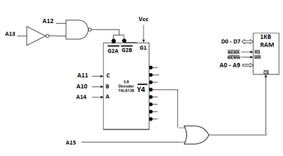
Figure 2
For the memory interface shown in Figure 3, determine the memory map.
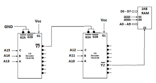
Figure 3
Identify the memory map and fold back space if the second decoder is eliminated in figure3 and (Y_7 ) ¯ pin of first decoder is connected directly (CS ) ¯of 1KB RAM.
Write a program to read the value from input port 30h and compare the received value with the data 60h. Place the received value in the registers as indicated below.
If value ?60h, store it in E.
If value = 60h, store it in H.
If value < 60h, store it in L.
b. The LOOP in the program of table 1 will be executed five times. Write the content of register A during every iteration.
| Label |
Instruction |
| |
LXI D, 057Bh |
| |
MOV A, E |
| LOOP: |
SUI 04h |
| |
INR A |
| |
DCR D |
| |
JNZ LOOP |
c. Using the concept of stack, write a program to store the contents of the flag register and accumulator in memory location 4000h and 4001h respectively.
3. a. Calculate the delay generated by the subroutine given in table 2. Assume the system clock period as 0.35μs.
| Label |
Instruction |
T-states |
| |
LXI D, 7200h |
10 |
| |
NOP |
4 |
| |
NOP |
4 |
| DELAY |
DCX D |
6 |
| |
NOP |
4 |
| |
MOV A,D |
4 |
| |
ORA C |
4 |
| |
JNZ DELAY |
7-Oct |
b. What will be value of maximum and minimum delay possible to generate from the subroutine given in table 2?
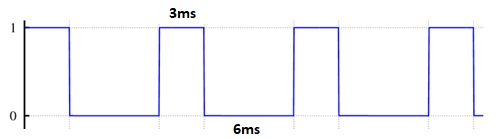
c. Write a program for 8255 PPI to generate the rectangular waveform as shown in figure 4. Assume that the delay subroutine of 3ms is available for the access and can be called as per the need.
d. If a 4KB RAM interfaced with microprocessor has the final address of 5D7Eh, find the starting address.
4. a. Analyze the program given in table 3 and answer the questions given below.
i. What is the value of SP register after execution of line 3
ii. In which memory location the value of register L will be stored
iii. What is the value of SP register after execution of line 5
iv. In which memory location the value of register B will be stored
v. What is the value of register A after the execution of line 7
vi. What is the value of S flag after the execution of line 7
b. Assuming the microprocessor is completing an RST 7.5 interrupt request; write a program to see if RST 5.5 is pending.
If it is pending, enable RST 5.5 without affecting any other interrupts, Otherwise return to the main program.
c. Write a program to check if the AC flag is set or reset after certain arithmetic operation. If it set then send EEh to output port or else send 00h. Call the subroutine named COPY to get the value of flag register in Accumulator.
Attachment:- Microprocessors and Interfacing.rar