Reference no: EM131069795
Electrical model of a cascade connection of two identical CMOS inverter circuits is shown in Figure 1(a), and the layout of one of the inverters is shown in Figure 1(b).
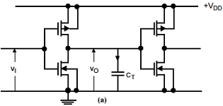
Figure 1(a)
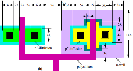
Figure 1(b)
The circuit of Figure 1 has been manufactured using an n-well process with the following parameter values:
a)whole IC
- electron/hole mobility µn= 0.057 m2/Vs - µp= 0.03 m2/Vs
- threshold voltage VTN = 0.25 VSS - VTP = -0.3 VSS
- body doping NAb = 4.1020accptor atoms/m3
- n-well doping NDw = 5.1021donor atoms/m3
- n-diffusion doping NDd = 1022donor atoms/m3
- p-diffusion doping NAd = 1023acceptor atoms/m3
- thinox thickness tox=0.08 µm
- junction depth Xj = 0.6 µm
- lateral diffusion LD = 0.6 µm
- minimum feature size λ= 0.6µm
- dielectric constant of vacuumεo= 8.85.10-12 F/m - intrinsinc concentr. of Si ni=1.5⋅1016/m3
- dielectric constant of Si εSi =11.7 εo -- dielectric constant of SiO2 εox=3.97 εo
b) pull-down transistor
- channel length LN = 2λ
- channel width WN = 4λ
c) pull-up transistor
- channel length LP = 2λ
- channel width WP = 8λ.
d) power supply voltage VDD = 5V
Assignment: Calculate the total lumped parasitic capacitance CT at the interconnection node of two inverters shown in Figure 1. Show the following steps of the solution process.
A. Calculate electrical parameters of the NMOS and PMOS transistors
A1. Drain diffusion-to-body junction capacitancies per unit area
A1.1 n-channel transistor bottom of drain diffusion to bulk pn+ junction
A1.11builtin potential:
A1.12 zero-bias depletion-layer capacitance per unit area Cjon (CJ).
A1.2 p-channel transistor bottom of drain diffusion to bulk p+n junction
A1.21 built in potential:
A1.22 zero-bias depletion-layer capacitance per unit area Cjop (CJ).
A2. Zero-bias depletion-layer capacitance per unit length of diffusion perimeter (CJSW) for the drainsidewall
n+p+ junctions, assuming that field doping is ten times higher than body doping.
A2.1 n-channel transistor
A2.2 p-channel transistor
A3. "Thinox" (gate to channel) capacitance per unit area Cox.
A4. Gate to source, and gate to drain overlap capacitances per unit of gate width CGSO and CGDO,
B. Layout dimensions of the NMOS and PMOS transistors
B1. Pull-down transistor
B1.1 drain and source areas,
B1.2 drain and source perimeters in cut-off region of operation,
B2. Pull-up transistor
B2.1 drain and source areas,
B2.2 drain and source perimeters in cut-off region of operation, when they are the greatest,
C. Parasitic transistor capacitances that affect propagation delays
C1. Total transistor capacitances at an inverter's output CTO
C1.11 Total drain-to-body junction capacitance value is,
C1.12 Gate-to-drain ovrlap capacitance value is,
C1.2 p-channel transistor
C1.21 Total drain-to-body junction capacitance value is,
C1.22 Gate-to-drain overlap capacitance value is,
C1.3 Total parasitic transistor capacitance seen from the inverter's output, CTO,
C2. Total transistor capacitance at the inverter's input CTI
C2.1 Gate-to-channel capacitance of the n-channel transistor,
C2.2 Gate-to-channel capacitances of the p-channel transistor,
C2.3 The total capacitance at the inverter's input CTI is then,
C3. The total lumped capacitance at the interconnection node CT