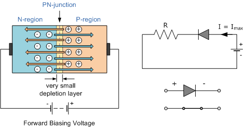
Forward Biased Junction Diode
When the diode is connected in a Forward Bias condition, the negative voltage is applied to N- type material and a positive voltage is applied to P-type material. If the external voltage becomes greater than value of the potential barrier, approximately 0.7 volts for the silicon and 0.3 volts for germanium, potential barriers opposition will be overcome and current will begin to flow. This is because the negative voltage pushes or repels electrons towards junction giving them the energy to cross over and combine with holes being pressed in the opposite direction towards the junction by positive voltage. This results in a characteristics curve of zero current flowing up to this voltage point, known as the "knee" on the static curves and then a high current flow through diode with the little increase in the external voltage as shown in the figure below.
Forward Characteristics Curve for a Junction Diode
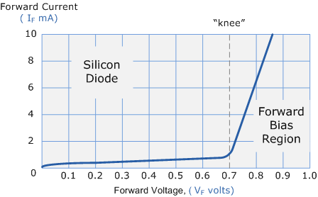
Application of the forward biasing voltage on junction diode results in the depletion layer becoming extremely thin and narrow which represents a low impedance path through the junction thus allowing high currents to flow. The point at which the sudden increase in the current takes place is represented on static I-V characteristics curve above as "knee" point.
Forward Biased Junction Diode showing a Reduction in the Depletion Layer
This particular condition represents the low resistance path through PN junction permitting very large currents to flow through diode with only a small increase in the bias voltage. The actual potential difference across the junction or diode is kept constant by action of the depletion layer at about 0.3v for germanium and about 0.7v for silicon junction diodes. Since the diode can conduct "infinite" current above this knee point as it effectively becomes a short circuit, therefore resistors are used in series with the diode to limit its current flow. Exceeding its maximum forward current specification causes the device to dissipate more power in the form of heat than it was designed for resulting in a very quick failure of the device.
Email based Electronics Devices and circuits assignment help - homework help at Expertsmind
Are you searching Electronics Engineering assignment help expert for help with Forward Biased Junction Diode questions? Forward Biased Junction Diode topic is not easier to learn without any external help? We at www.expertsmind.com offers free lecture notes for Electronics Devices and circuits assignment help and Electronics Devices and circuits homework help. Live tutors are available 24x7 hours for helping students in their Forward Biased Junction Diode related problems. We provide step by step Forward Biased Junction Diode question's answers with 100% plagiarism free content. We prepare quality content and notes for Forward Biased Junction Diode topic under Electronics Devices and circuits theory and study material. These are avail for subscribed users and they can get advantages anytime.
Why Expertsmind for assignment help
- Higher degree holder and experienced experts network
- Punctuality and responsibility of work
- Quality solution with 100% plagiarism free answers
- Time on Delivery
- Privacy of information and details
- Excellence in solving electronics engineering questions in excels and word format.
- Best tutoring assistance 24x7 hours