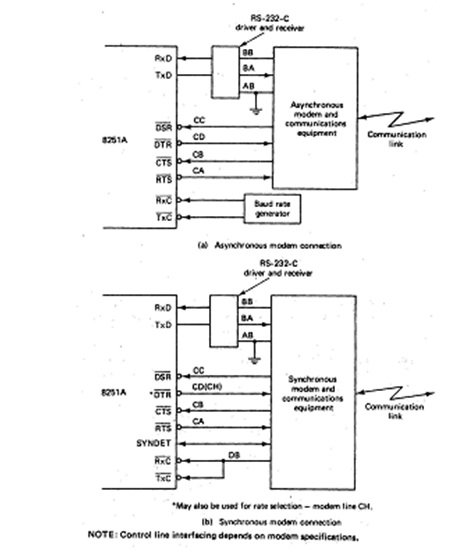
Typical link to modems for synchronous and asynchronous transmissions are shown in Figure. With regard to the synchronous connections it is consider that the timing is controlled by the modem and its related communications equipment. Also, if this equipment is utilized to detect the sync character(s) at the beginning of a received message, then it might inform the 8251A of its success over the SYNDET line. Otherwise, if 8251A searches for the sync character(s), then it may use the SYNDET line as an output to tell the modem that the sync character(s) has been found. To satisfy the RS-232-C standard, receivers and drivers are required to convert the TTL-compatible signals at TxD and RxD to the right voltage levels.
A program sequence which starts the mode register and gives a command to enable the transmitter and start an asynchronous transmission of 7-bit characters followed by an even-parity bit and 2 stop bits is:
MOV AL, 11111010B OUT 51H, AL
MO AL, 00110011B OUT 51H, AL
This sequence assumes that the mode and control registers are at address 511-1 and the clock frequencies are to be 16 times the corresponding baud rates. The sequence is as follow:
MOV AL, 00111000B OUT 51H, AL
MOV AL, 16H OUT 51H, AL OUT 51H, AL
MOV AL, 10010100B OUT 51H, AL
would cause the similar 8251A to be put in synchronous mode and to begin searching for two successive ASCII sync characters. The characters are to consist of seven data bits and an even parity bit, but of course, there will be no stop bits. The format of the status register is described in the given figure. Bits 1, 2, and 6 reflect the signals on the RxRDY, TxE, and SYNDET pins. TxRDY denoted that the data-out buffer is Empty. This bit is not affected by the CTS input pin or the TxEN control bit Unlike the TxRDY pin. RxRDY indicates that a character has been received and is ready to be input to the processor. Either the TxRDY and RxRDY bits may be used for programmed I/O or the signals on the corresponding pins may be linked to interrupt request lines to provide for interrupt I/O. The TxRDY bit is automatically cleared when a character is available for transmitting and the RxRDY bit is automatically cleared when the character that set it is input by the processor. Bit 2 denoted that the transmitter shift register is waiting to be sent a character from the data-out buffer register. During synchronous transmissions, whereas this bit is set, the transmitter will take its data from the sync character registers till data are put in the data-out buffer register. Bits 4, 3, and 5 indicate overrun, parity, and framing errors, respectively. When an error is detected, the bit having the corresponding error type will be set to one. If the complement of the DSR pin is linked to the Data Set Ready (CC) line, then bit seven reflects the state of the modem and is valued 1 when the modem is turned on and is in its data mode.
Figure gives a program sequence which uses programmed I/O to input 80 characters from the8251A, whose address of data buffer register is 0050, and put them in the memory buffer starting at LINE. The inner loop continually tests the RxRDY bit till it is set by a character being put in the data-in buffer register. Then the newly arrived character is moved to the buffer and the error bits are checked. If the present character arrived before the previous character was a parity or input or framing error occurred during the transmission, then the input ceases and a call is made to an error routine that would presumably examine the particular error bits, print an suitable message, and clear the error bits.
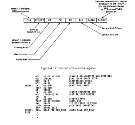
Because inputting a character automatically resets the RxRDY bit, unless another character is received before the inner loop is re entered, the inner loop might be cycle till the RxRDY bit is reset to one by the next incoming character. If the incoming characters have less than eight bits, MSBs, which are unused, in the data buffer register are always being 0. The parity bit is also not passed to the processor and examine for parity errors may only be made by checking the parity error bit in the status register. On output, if a character is less than eight bits long, the unrequited MSBs in the data-out buffer register are avoided.