Machine coding the programs-microprocessor, Assembly Language

Assignment Help:

Machine Coding the Programs

So far we have describe five programs which were  written  for hand coding  by a programmer. In this, we will now have a deep look at how these programs may be  translate to machine codes. In Appendix, the instruction set along with the Appendix is presented. This Appendix is self-explanatory to hand code mostly of the instructions. The V,S W, D, MOD, REG  and R/M  fields are appropriate decided depending upon the data types, addressing mode and the registers  used. The table shows the details about how to select these fields.

Most of the instructions either have particular opcodes or they may be decided only by setting the V,S, W, D, REG, MOD and R/M fields suitably but the critical point is  the calculation of jump addresses for intra segment branch instructions. Before beginning the coding of call or jump instructions, we will see some simpler coding examples.

Example :

MOV BL, CL

For hand coding this instruction, first we will have to note down the following features.

(i) It sets in the register/memory to/from register format.

(ii) It is an 8-bit operation.

(iii) BL is the destination register and CL is a source register.

Now from the feature (i) by using the Appendix, the op code format is given below.

1485_mcp.jpg

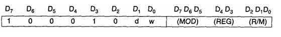
If d =1, then transformation of data is to the register shown by the REG field, for example the destination is a register (REG). If d = 0, the source is a register shown by the REG field. It is an 8-bit operation, therefore w bit is 0. If it had been a 16-bit operation, the w bit would have been 1.From referring to given table to search the REG to REG addressing in it, for example the last column with MOD 11. According to the Appendix when MOD is 11, the R/M field is treated as a REG field. The REG field which is used for source register and the R/M field are used for the destination register, if d is 0. If d =1, the REG field is utilized for destination and the R/M field is used to indicate source. the complete machine code of this instruction comes out to be now.

code    dw       MOD   REG    R/M

MOV BL, CL 1 0 0 0 1 0 0 0     1   1   001    0 1 1= 88 CB


Related Discussions:- Machine coding the programs-microprocessor

#title:Shifitng of memory, Ask 2. Exchange higher byte of AX and higher byt...

Ask 2. Exchange higher byte of AX and higher byte of BX registers by using memory location 0160 in between the transfer. Then stores AX and BX registers onto memory location 0174 o

Assignment, Write an assembly program that adds the elements in the odd ind...

Write an assembly program that adds the elements in the odd indices of the following array. Use LOOP. What is the final value in the register?

Third generation microprocessor, III rd Generation Microprocessor: T...

III rd Generation Microprocessor: The single 3rd generation microprocessor chip having 64-pins began with the introduction of 16-bit Intel 8086 in 1978. The other essential

Sequence of interrupts, As an instance of the normal priority mode, imagine...

As an instance of the normal priority mode, imagine that initially AEOI is equal to 0 and all the ISR and IMR bits are clear. Also consider that, as shown in given figure, requests

Length-assemblers directive-microprocessor, LENGTH : Byte Length of a Labe...

LENGTH : Byte Length of a Label: This directive is not available in MASM. This is used to mention to the length of a data array or a string. MOV CX. LENGTH ARRAY This sta

Program to convert decimal to binary number, Program is written but has err...

Program is written but has errors returning values from the procedure.

Physical memory mapped and port input output-microprocessor, Physical Memor...

Physical Memory Mapped I/O and Port I/O : CPU controlled I/O comes in 2 ways. Simply the difference is whether we utilize the normal memory addresses for I/O, this is mention

Cache components-microprocessor, Cache components The cache sub-system ...

Cache components The cache sub-system may be divided into 3 functional blocks: Tag RAM, SRAM and theCache Controller. In real designs, these blocks can be implemented  by multi

Program, Write an application that does the following: (1) fill an array wi...

Write an application that does the following: (1) fill an array with 50 random integers; (2) loop through the array, displaying each value, and count the number of negative values;

Write Your Message!

Captcha
Free Assignment Quote

Assured A++ Grade

Get guaranteed satisfaction & time on delivery in every assignment order you paid with us! We ensure premium quality solution document along with free turntin report!

All rights reserved! Copyrights ©2019-2020 ExpertsMind IT Educational Pvt Ltd