Draw the circuit of A/D converter using a V/F converter, Computer Engineering

Assignment Help:

Draw the schematic circuit of an Analog to Digital converter using Voltage-to Frequency conversion and explain its principle of operation. Draw its relevant Waveforms.

Ans:

Analog to Digital Converter Using Voltage-to-Frequency Conversion: An analog voltage can be converted into digital form by producing pulses whose frequency is proportional to the analog voltage. These pulses are counted by a counter for a fixed duration and the reading of the counter will be proportional to the frequency of the pulses and hence to the analog voltage.

A voltage-to-frequency converter is shown in Fig. (a). The analog voltage Va is applied to an integrator whose output is applied at the inverting input terminal of a comparator. The non-inverting input terminal of the comparator is connected to a reference voltage -VR.

Initially, the switch S is open and the voltage vo decreases linearly with time (vo = Vat/τ ) which is shown in Fig. 10(b). When the decreasing vo reaches -VR at t =T, the comparator output  VC   goes  HIGH.  This  is  used  to  close  the  switch  S  through  a  monostable multivibrator. When the switch S is closed, the capacitor C discharges, thereby returning the integrator output vo  to 0. Since the pulse width of the waveform VC is very small, therefore, a monostable multivibrator is used to keep the switch S closed for a sufficient time to discharge the capacitor completely. The rate at which the capacitor discharges depends upon the resistance of the switch.

Let the pulse width of the monostable multivibrator be Td. Therefore, the switch S remains closed for Td after which it opens and vo starts decreasing again.

If the integration time T >> Td, the frequency of the waveforms Vo and VC is given by

 f = 1/( T + Td)  ≅  1/T = (1/ τ) (Va/VR)

Therefore we get an output waveform whose frequency is proportional to the analog input voltage. Using the voltage-to-frequency (V/F) converter an A/D converter is demonstrated in Fig.(c). The output of the voltage-to-frequency converter is applied at the clock (CK) input of a counter throughout an AND gate. For a fixed time interval T1, the AND gate is enabled. The reading of the counter at t = T1 is specified by

n =  fT1 =  (1/ τ) (Va/VR) T1  that is proportional to Va

558_Logic diagram of Voltage-to-Frequency Converter.png

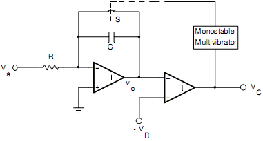
Fig.(a) Logic diagram of Voltage-to-Frequency Converter


1904_Waveforms of Voltage-to-Frequency Converter.png

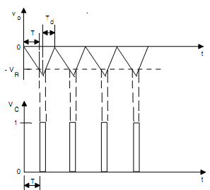
Fig.(b) Waveforms of Voltage-to-Frequency Converter


131_Schematic circuit of AD converter using a VF converter.png

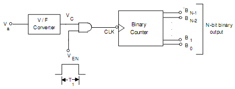
Fig.(c) Schematic circuit of A/D converter using a V/F converter


Related Discussions:- Draw the circuit of A/D converter using a V/F converter

Explain why the ROM is a volatile memory, Is the ROM a volatile memory? Exp...

Is the ROM a volatile memory? Explain Ans. No, ROM is a Non-Volatile memory. Programming of ROM includes making of the needed  interconnections at  the time of fabrication and

What is the difference among choice and list, A Choice is displayed in a co...

A Choice is displayed in a compact form that needs you to pull it down to see the list of available choices and only one item may be selected from a choice. A List may be shown in

What is modem?, A device, usually linked to a serial port of a computer, th...

A device, usually linked to a serial port of a computer, that transfer data over regular phone lines. Modem stands modulator demodulator; it changes a digital stream of data into s

Avoiding local minima of multi-layered networks, Avoiding Local Minima of m...

Avoiding Local Minima of multi-layered networks-Artificial intelligence : The error rate of multi-layered networks over a training set could be calculated as the number of mis

Explain the test instruction, Explain the TEST instruction TEST instru...

Explain the TEST instruction TEST instruction performs the AND operation. The difference is that AND instruction changes the destination operand whereas TEST instruction doesn

Marked statement is implemented , Consider the ReadRear Java method (a)...

Consider the ReadRear Java method (a) Illustrate pictures that explain the data structure every time a checkpoint is reached for the problems of sizes one, two, three and four s

Explain the meaning of listen socket primitive, Explain the meaning of L...

Explain the meaning of LISTEN socket primitive The listen Primitive: After identifying a protocol port a server should instruct the operating system to place a socket

Library markup language, 1. Design a DTD for a new XML application called L...

1. Design a DTD for a new XML application called Library Markup Language (LibML) appropriate to capture the list of your items of collection . Put the DTD into a file named librar

Write the truth table of NOR gate, Write the truth table of NOR gate. Ans...

Write the truth table of NOR gate. Ans. The truth table for NOR gtae is shown below:

What is open database connectivity, What is Open Database Connectivity (ODB...

What is Open Database Connectivity (ODBC) It happens that in addition to conventional or most popular database management systems, many companies go for proprietary software c

Write Your Message!

Captcha
Free Assignment Quote

Assured A++ Grade

Get guaranteed satisfaction & time on delivery in every assignment order you paid with us! We ensure premium quality solution document along with free turntin report!

All rights reserved! Copyrights ©2019-2020 ExpertsMind IT Educational Pvt Ltd