Reverse Biased Junction Diode
When the diode is connected in a Reverse Bias condition, a positive voltage is applied to N- type material and a negative voltage is applied to P-type material. The positive voltage which is applied to N-type material attracts electrons towards positive electrode and away from the junction, while holes in P-type end are also attracted away from the junction towards negative electrode. The net result is that the depletion layer grows wider because of a lack of electrons and holes and presents the high impedance path, almost an insulator. The result is that a high potential barrier is created hence preventing current from flowing through semiconductor material.
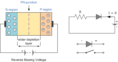
Reverse Biased Junction Diode showing an Increase in the Depletion Layer
This condition shows a high resistance value to PN junction and practically zero current flows through junction diode with an increase in bias voltage. However, small leakages current do not flow through the junction which can be measured in microamperes, (μA). One final point, if the reverse bias voltage Vr applied to the diode is increased to a sufficiently high enough, it will cause PN junction to overheat and fail because of the avalanche effect around junction. This can cause the diode to become shorted and results in the flow of maximum circuit current, and this shown as a step downward slope in reverse static characteristics curve below.
Reverse Characteristics Curve for a Junction Diode
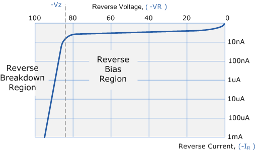
At times this avalanche effect has practical applications in the voltage stabilizing circuits where the series limiting resistor is used with diode to limit this reverse breakdown current to preset maximum value thus producing a fixed voltage output across the diode. These types of diodes are commonly called as Zener Diodes.
Email based Electronics Devices and circuits assignment help - homework help at Expertsmind
Are you searching Electronics Engineering assignment help expert for help with Reverse Biased Junction Diode questions? Reverse Biased Junction Diode topic is not easier to learn without any external help? We at www.expertsmind.com offers free lecture notes for Electronics Devices and circuits assignment help and Electronics Devices and circuits homework help. Live tutors are available 24x7 hours for helping students in their Reverse Biased Junction Diode related problems. We provide step by step Reverse Biased Junction Diode question's answers with 100% plagiarism free content. We prepare quality content and notes for Reverse Biased Junction Diode topic under Electronics Devices and circuits theory and study material. These are avail for subscribed users and they can get advantages anytime.
Why Expertsmind for assignment help
- Higher degree holder and experienced experts network
- Punctuality and responsibility of work
- Quality solution with 100% plagiarism free answers
- Time on Delivery
- Privacy of information and details
- Excellence in solving electronics engineering questions in excels and word format.
- Best tutoring assistance 24x7 hours