Signal descriptions of 8086 : described below are common for the maximum andminimum mode bothdata lines
AD15 -AD0: These are the time multiplexed andmemory I/O address. Address remains on the lines during T1 state, while the data is available on the data bus during T3, T2, Tw and T4. Here T4, T3, T2, T1 and Tw are the clock states of a machine cycle. Tw is a wait state. These lines are active high and float to a tristate during local bus andinterrupt acknowledge hold acknowledge cycles.
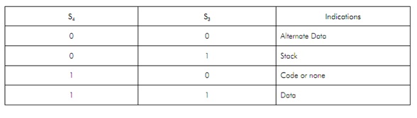
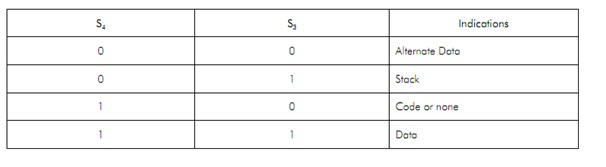
A19/S6, A18/S5, A17/S4, and A16/S3: These are the time multiplexed address and status lines. During T1, these are the most important address lines for memory operations. These lines are lowduring l/O operations. During I/O operations ormemory, status information is existing on those lines forT1 T2, T3, T4 and Tw. The status of the interrupt enable flag bit (displayed on S5) is updated at the starting of each clock cycle. The S3 and S4combineddenoted which segment register is presently being used for memory accesses as shown in Table These lines float to tri-state off (tristated) during the local bus hold acknowledge. The status line S6 isalways low (logical). The address bits are separated from the status bits by using latches controlled by the ALEsignal.
BHE/S7-Bus High Enable/Status: The bus high enable signal is utilized to indicate the transfer of data over the higher order (D15-D8) data bus as shown in Table. It goes low for the data transfers during D15-D8, and is utilized to derive chip selects ofperipherals or odd address memory bank. BHE is low during T1 forwrite,read and interrupt acknowledge cycles, whenever one byte is to be transferred on the higher byte of the data bus. The status information is accessduring T1, T2, T3 and T4. The signal istri statedand active low during'hold'. It is low during T1 for the first pulse of the interrupt acknowledges cycle.
RD-Read: Read signal, when low, denoted the peripherals that the processor is performing an I/O read operation ormemory. RD is active low and shows the state for T2, T3, and Tw of any read cycle. The signal remains tristated during the 'hold acknowledge'.
READY: This is the acknowledgement from the memoryor slow devices that they have completed the data transfer. By the devices the signal made available is synchronized by the 8284A clock generator to supply ready input to the 8086. That signal is active high.
INTR-Interrupt Request: This is a level triggered input. It is sampled during the last clock cycle of every instruction to decide the availability of the request. If interrupt request is not served,the processor enters the interrupt acknowledge cycle. It may be internally masked by resetting the interrupt enable flag. This signal is internally synchronized and active high.
TEST: This input is checked by a 'WAIT' instruction. If the TEST input goes low, execution willcontinue else the processor remains in an idle state. Internally the input issynchronized during each clock cycle on leading edge of clock.
NMI-Non-mask able Interrupt: This is an edge-triggered input that causes a Type2 interrupt. Internally the NMI is not mass able by software. A transition from low to high initiate the interrupt response at the end of the current instruction.Internallythis input is synchronized.
RESET this input causes the processor to close the current activity and start execution from FFFFOH. The signal is active high and might be active for at least 4 clock cycles. It restarts execution while the RESET returns low. Also, RESET is internally synchronised.
CLK-Clock Input: The clock input provides the basic timing for bus control activity andprocessor operation. It's an asymmetric square wave with 33% duty cycle. The range of frequency for different 8086 versions is from 5MHz to l0MHz.
Vcc +5V: power supply for the operation of the internal circuit. GND: ground for the internal circuit.
MN/MX: The logic level at this pin decides whether the processor is to operate in either maximum (multiprocessor) mode orminimum (single processor)