Opcode :
The opcode generally appear in the first byte.but in a few instructions, a register objective is in the first byte and few other instructions may have their 3-bits of opcode in the second byte. The opcodes contain single bit indicators. Their definitions and significance's are described below.
- W-bit: This indicates whether the instruction is to operate above 8-bit or 16-bit data/operands. If bit is 0, the operand is of8-bits and if W is equal to I, the operand is of 16-bits.
- D-bit: This is valid in case of double operand instructions. One of the operands might be a register indicated by the REG field. The register indicated by REG is source operand ifD value is 0; else, it is a destination operand.
- S-bit: This bit is known as sign extension bit. The S bit is utilized along with W-bit to show the type of the operation. For an example
a) 8-bit operation with 8-bit immediate operand is specified by S = 0, W = 0;
b) 16-bit operation with 16-bit immediate operand is specified by S = 0, W = 1 and
c) 16-bit operation with a sign extended immediate data is given by S = 1, W = 1
- V-bit: This is utilized in case ofrotate and shift instructions. This bit is set with the value 0, if shift count is 1 and it is set for value 0, if CL contains the shift count.
- Z-bit: This bit is utilized by REP instruction to control the loop. If Z bit is equivalent to I, the instruction with REPprefix is executed till the 0 flag matches the Z bit.
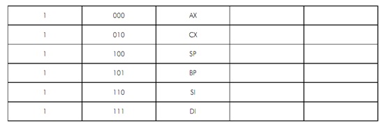
The REG code of the different registers (either as destination operandsor source) in the op code byte is assigned with binary codes. The segment registers are just four in number hence 2 binary bits will be enough to code them. The other registers are eight in number, so at least 3-bits will be required for coding them. To permit the use of 16-bit registers as two 8-bit registers they are coded with W bit as described in Table
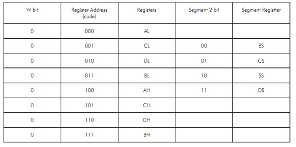
Please note that generally all the addressing modes contain DS as the default data segment. Though, the addressing modes by using SP and BP have SS as the default segment register.
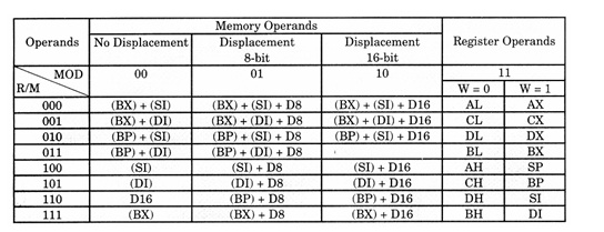
To search theR/M and MOD fields of a specific instruction, one should first decide the addressing mode of the instruction. The addressing mode depends on the suggestionand operands how the effective address can be computed for locating the operand, if it lies into the memory. The different addressing modes of the 8086 instructions are listed in given table. The R/M column and addressing mode row element indicate the R/M field, whereas the addressing mode column indicates the MOD field.
When a data is to be indicated as an operand and, DS: default data segment register. CS is the default code segment register for the purpose of storing program codes (executable codes). SS is the default segment register for thecause of stack data accesses and operations. ES is a default segment register for the destination data storage. All the segments existing (defined in a particular program) may be written or read as data segments by newly defining the data segment as needed. There is no physical difference in the memory structure or no physical separation between the segment areas. They might / might not overlap with each other.