Explain classification of energy band materials, Electrical Engineering

Assignment Help:

With the help of energy bands explain how conduction takes place in conductors, semiconductors and insulators.

On the basis of energy band materials are categorized as insulators, conductors and semiconductors.

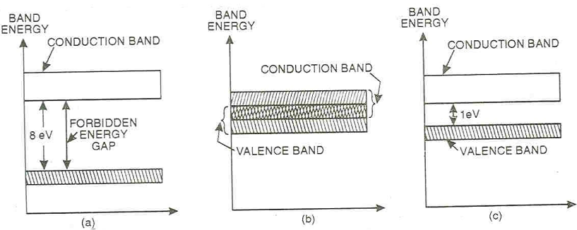
Insulators: Substance as wood, glass, that do not permit the passage of current through them is termed as insulators. The valence band of these substances is full while the conduction band is fully empty. The forbidden energy gap among valence band and conduction band is very large (8ev) as demonstrated in the figure (a). Thus, a large amount of energy that is a very high electric field is needed to push the valence electrons to the conduction band. It is the reason, why such materials under ordinary conditions do not conduct at all and are designated like insulators.

Conductors: Substances as copper, aluminium and silver that permit the passage of current through them are conductors. The valence band of such substances overlaps the conduction band as demonstrated in figure (b). Because of this overlapping, a large number of free electrons are available for conduction. It is the purpose, why a slight potential difference applied across them causes a heavy flow of current throughout them.

Semiconductors: Substances as carbon, germanium and silicon that electrical conductivity lies in among the conductors and insulators are termed as semiconductors. The valence band of such substances is approximately filled, but the conduction band is approximately empty. The forbidden energy gap between valence and conduction band is very small (1ev) as shown in figure (c). Thus comparatively a smaller electric field is needed to push the valence electrons to the conduction band. It is the reason, why these materials under ordinary conditions do not conduct current and behaves as an insulator. Even though at room temperature, while some heat energy is imparted to the valence electrons, some of them cross over to the conduction band imparting minor conductivity to the semiconductors. Since the temperature is raised, more valence electrons cross over to conduction band and conductivity of the material raises. Therefore these materials have negative temperature co-efficient of resistance.

497_Energy Band Diagrams.png

Energy Band Diagrams


Related Discussions:- Explain classification of energy band materials

General equivalent circuits, What we have seen for practical power supplies...

What we have seen for practical power supplies applies to any  electrical circuit provided it contains only linear components

Solar steam power generator, This project is about another particular appli...

This project is about another particular application of a particular embodiment of the patent: A Long Stroke Steam Engine using Solar Generated Steam. The machine elements such as

Accidents, what are accidents in an organisation

what are accidents in an organisation

What are the different parameters of jfet, Q. What are the different parame...

Q. What are the different parameters of jfet ? A bipolar junction transistor (BJT) is a current controlled device that is output characteristics of the device are controlled by

Illustrate the working of full wave rectifier, Illustrate the working of fu...

Illustrate the working of full wave rectifier using bridge rectifier. How is it different from centre tapped Rectifier ? Illustrate Avalanche and Zener breakdown. Draw & explain

Explain two types of materials that are formed after doping, Explain the tw...

Explain the two types of materials that are formed after doping. Depending on the impurity added, extrinsic semiconductors can be then subdivided in two types of class: N-ty

Sectoral overview and enabling framework, Sectoral Overview and Enabling Fr...

Sectoral Overview and Enabling Framework Previously, you have studied about several Acts and Policies relevant to the power sector, their aims, main features and implications

MATLAB support for fault analysis in transmission lines, The devices in pow...

The devices in power system shown in Figure 2 have the following ratings: G1 : 100 MVA, 13.8 kV grounded Y, X” = 0.15 pu, X2 = 0.015 pu Xo = 0.05 pu G2 : 50 MVA, 20.0 kV grounded

Logic Gates, XOR gate BY using NAND gate Only

XOR gate BY using NAND gate Only

Superposition, advantages and disadvantaages of superposition

advantages and disadvantaages of superposition

Write Your Message!

Captcha
Free Assignment Quote

Assured A++ Grade

Get guaranteed satisfaction & time on delivery in every assignment order you paid with us! We ensure premium quality solution document along with free turntin report!

All rights reserved! Copyrights ©2019-2020 ExpertsMind IT Educational Pvt Ltd