Explain by using a circuit diagram a darlington pair, Electrical Engineering

Assignment Help:

Q. Explain by using a circuit diagram, a ‘Darlington Pair'. Mention its advantages?

THE DARLINGTON PAIR : This is a very special way of direct coupling of two transistors. The two are connected with their collectors to the same point. The emitter of the first transistor is connected directly to the base of the next.

1771_Explain by using a circuit diagram a darlington pair4.png

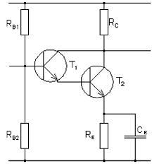
A common emitter amplifier with Darlington. The two transistors are interconnected with their collectors, while the emitter of the first transistor feeds into the base of the second. An emitter resistor (RE1) is sometimes used for the first transistor to achieve faster switching.


351_Explain by using a circuit diagram a Darlington Pair1.png


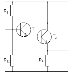
Common collector amplifier with Darlington. With this amplifier extremely high input resistances and extremely low output resistances can be achieved.


The advantage of the Darlington is the VERY HIGH CURRENT GAIN, which is the product of the current gains of the individual transistors. For ? values up to 20 000 can be achieved.

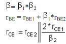
The Darlington has three terminals, like a normal transistor. In fact it can be considered as ONE transistor. The characteristics or this Darlington transistor can then be expressed in terms of the characteristics of the individual transistors:


1129_Explain by using a circuit diagram a Darlington Pair2.png


Darlington transistors are available in normal transistor housings, e.g. BC517 or BD675.

2419_Explain by using a circuit diagram a Darlington Pair3.png


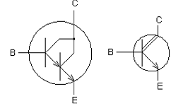
A Darlington pair in one housing. As for normal transistors, the terminals are called collector, base and emitter.

Different circuit symbols are used for Darlington transistors. A transistor amplifier stage using a Darlington pair is normally considered as ONE amplifier stage, although two transistors are used.


Related Discussions:- Explain by using a circuit diagram a darlington pair

Dc simulation component, Once you are happy with the biasing components you...

Once you are happy with the biasing components you will need to disable the DC simulation component and enable the SP component. (Right click the component and then select the "com

Reduce the circuit to a thevenin and a norton equivalent, Q. Reduce the cir...

Q. Reduce the circuit of Figure to a Thévenin and a Norton equivalent circuit with respect to terminals a-b.

Draw circuit diagrams and show polarity markings, Q. Two single-phase trans...

Q. Two single-phase transformers, each rated 2400: 120-V, are to be interconnected for (a) 4800:240- V operation, and (b) 2400:120-V operation. Draw circuit diagrams and show polar

Obtain the laplace transform of the waveform, Q. Use MATLAB to obtain the L...

Q. Use MATLAB to obtain the Laplace transform of the waveform f(t) = [200t e -25t + 10 e -50t sin(25t)]u(t) which consists of a damped ramp and a damped sine. Also show the

Diatomic molecules in three dimensions, Consider the open rotation of a dia...

Consider the open rotation of a diatomic molecule consisting of two atoms of mass and respectively divided by a distance presume that the molecule is rigid with center of mass fixe

Find the current by means of mesh-current analysis, For the network shown i...

For the network shown in Figure, find the current delivered by the 10-V source and the voltage across the 3- resistor by means of mesh-current analysis.

Find the speed of the motor, Q. A 10-kW, 230-V shunt generator, with an arm...

Q. A 10-kW, 230-V shunt generator, with an armature-circuit resistance of 0.1  and a field- circuit resistance of 230 , delivers full load at rated voltage and 1000 r/min. If the

1- phase full bridge inverter with r- load , 1- phase  Full Bridge Invert...

1- phase  Full Bridge Inverter with R- Load 1-phase full  bridge inverter with resistive load R i it has  advantage over 1-? half  bridge  inverter that it does  not require

Transistor terminals in bjt, Q. Transistor terminals in BJT ? BJTS have...

Q. Transistor terminals in BJT ? BJTS have three terminals namely base terminal, emitter terminal and collector terminal .The emitter layer is a source of charge carriers and i

Write Your Message!

Captcha
Free Assignment Quote

Assured A++ Grade

Get guaranteed satisfaction & time on delivery in every assignment order you paid with us! We ensure premium quality solution document along with free turntin report!

All rights reserved! Copyrights ©2019-2020 ExpertsMind IT Educational Pvt Ltd