Depletion type mosfet, Electrical Engineering

Assignment Help:

Depletion type MOSFET

The channel is of silicon. It can be two type of channel that is an n-type or p-type channel; it is still mostly silicon. After that, we take note that silicon dioxide is simply glass that is a good insulator. Thus we can form a thin layer of silicon dioxide together one surface of the channel, and then lay our metal gate region down over the glass. The result is displayed in the figure.

140_Depletion type MOSFET 1.png

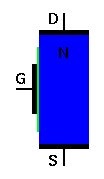
Sometimes this device is termed as an insulated-gate field effect transistor, or IGFET. More generally, noting the construction of the gate, it is termed as a metal-oxide-semiconductor FET, or MOSFET.

Without voltage applied to the gate (G) electrode, the channel really is only a semiconductor resistance, and will conduct current as per to the voltage applied in between source (S) and drain (D). There is no pn junction, thus there is no depletion region.

2352_Depletion type MOSFET 2.png

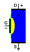
With a suitable voltage applied in between source and drain, current will flow via the channel, as a semiconductor resistance. Though, if we now apply a negative voltage to the gate, as displayed in figure, it will amount to a small negative static charge on the gate. This negative voltage will repel electrons, along with their negative charge, away from the gate. However, free electrons are the majority current carriers in the n-type silicon channel. Through repelling them away from the gate region, the applied gate voltage makes a depletion region around the gate area, so restricting the usable width of the channel just like the pn junction did. Since this sort of FET operates by creating a depletion region in an existing channel, it is termed as a depletion-mode MOSFET.


Related Discussions:- Depletion type mosfet

Control, The goal of this project is to model a system and to design a cont...

The goal of this project is to model a system and to design a controller for the system so that the closed-loop system performs satisfactorily.

Find the input resistance and output resistance, Quite often an amplifier i...

Quite often an amplifier is used as a component of an amplifier circuit. Consider the amplifier circuit shown in Figure, which contains an amplifier block as an internal component.

Can you explain noninverting amplifier, Q. Can you explain Noninverting Amp...

Q. Can you explain Noninverting Amplifier? It is called "noninverting" because there is no sign inversion. A typical circuit is shown in Figure. With a finite op-amp gain Ao,

Define the half duplex with respect to serial communication, With respect t...

With respect to serial communication define the half duplex. Half Duplex Transmission: A channel of half duplex can send and receive, but not at same time. It's like a one-la

Unijunction transistor, UniJunction Transistor: (abbreviated as UJT)...

UniJunction Transistor: (abbreviated as UJT), also called the double base diode, is a 2 layer, 3 terminal solid state switching device. The device has a unique characteristi

Find a local s-matrix for each triangle, Figure show two first-order triang...

Figure show two first-order triangular finite elements used to solve the Laplace equation for electrostatic potential. Find a local S -matrix for each triangle, and a global S -m

What do you mean by companding, Q. What do you mean by Companding? In o...

Q. What do you mean by Companding? In order to lower the crest factor of a waveform, so as to produce better performance, a process known as companding is used. It works like a

Write Your Message!

Captcha
Free Assignment Quote

Assured A++ Grade

Get guaranteed satisfaction & time on delivery in every assignment order you paid with us! We ensure premium quality solution document along with free turntin report!

All rights reserved! Copyrights ©2019-2020 ExpertsMind IT Educational Pvt Ltd