Define wilkes control unit, Computer Engineering

Assignment Help:

Q. Define Wilkes Control Unit?

Prof. M. V. Wilkes of the Cambridge University Mathematical Laboratory invented the term microprogramming in 1951. He offered a systematic alternative process for designing control unit of a digital computer. At the time of instruction executing a machine instruction, a sequence of transformations and transfer of information from one register in processor to another take place. These were also known as the micro operations. Due to the analogy between the executions of individual steps in a machine instruction to execution of individual instruction in a program. Wilkes introduced the idea of microprogramming. Wilkes control unitreplaces the combinational and sequential circuits of hardwired CU by a simple CU in conjunction with a storage unit which stores the sequence of steps of instruction which is a micro-program.

In Wilkes microinstruction has two main components:

a)  Control field thatdenotes the control lines which are to be activated and

b)  Address field that provides address of the subsequent microinstruction to be executed.

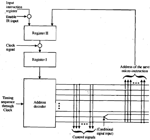
The figure below is an illustration of Wilkes control unit design. 
1315_Define Wilkes Control Unit.png

Figure: Wilkes Control Unit

The control memory in Wilkes control is organized like a PLA's like matrix made of diodes. This is partial matrix and comprises two components the control signals and address of the subsequent micro-instruction. Register I comprises the address of next micro-instruction which is one step of instruction execution, for illustration T1 in M1 or T2 in M2 etc. as in Figure below. On decoding the control signals are producedwhich cause execution of micro-operation(s) of that step. Additionally the control unit denotes the address of next micro-operation that gets loaded through register II to register I. Register I can also be loaded by register II and enable IR input control signal. This will pass address of first micro-instruction of execute cycle. At the time of a machine cycle one row of the matrix is triggered. The first portion of the row produces the control signals which control the operations of the processor. Second part produces the address of row to be selected in next machine cycle. 

At beginning of the cycle the address of the row to be selected is contained in register I. This address is input to decoder that is activated by a clock pulse.

This triggers the row of control matrix. Two-register arrangement is required as the decoder is a combinational circuit; with only one register output would become input at the time of a cycle. This can be an unstable condition because of repetitive loop.


Related Discussions:- Define wilkes control unit

Oo modelling, We might model such a scenario using three types of object: o...

We might model such a scenario using three types of object: one for Customers, one for BankAccounts and another for Transactions. In terms of data required, for Customers assume we

Explain concurrent sharing, Explain Concurrent sharing. Concurrent s...

Explain Concurrent sharing. Concurrent sharing: Some number of programs may share a file concurrently. While this is the case, this is essential to ignore mutual interferen

Explain the design reusability of verilog, Explain the Design reusability o...

Explain the Design reusability of Verilog There is no concept of packages in Verilog. Functions and procedures used within a model should be  defined  in  the  module.  To  mak

What is looping, What is looping Loop is a control structure used to do...

What is looping Loop is a control structure used to do repetitive operation. Some programs include repeating a set of instruction either a particular number of times or until a

Implement a memory management system , There should be 1 server thread and ...

There should be 1 server thread and N client threads, where N is supplied by the user as a command line argument. The server opens a file called "all_requests.dat", the file has

Illustrate cache dram, Q. Illustrate Cache DRAM? Cache DRAM (CDRAM) wh...

Q. Illustrate Cache DRAM? Cache DRAM (CDRAM) which is developed by Mitsubishi integrates a tiny SRAM cache (16Kb) on a generic DRAM chip. SRAM on the CDRAM can be used in two

Explain the term - integrity, Explain the term - Integrity In most c...

Explain the term - Integrity In most cases, corporate data should remain unchanged by third parties, so the system should be capable of ensuring that only authorised personn

Determine the simplified sop boolean expression, The Karnaugh map for a SOP...

The Karnaugh map for a SOP function is given below in figure. Determine the simplified SOP Boolean expression. Ans. F= B'C' + A'C'D + B'D'

How are the instructions executed and interpreted, Q. How are the instructi...

Q. How are the instructions executed and interpreted? All computers have a Unit which performs arithmetic and logical functions. This Unit is called as Arithmetic and Logic Uni

Write Your Message!

Captcha
Free Assignment Quote

Assured A++ Grade

Get guaranteed satisfaction & time on delivery in every assignment order you paid with us! We ensure premium quality solution document along with free turntin report!

All rights reserved! Copyrights ©2019-2020 ExpertsMind IT Educational Pvt Ltd