Define SR Flip Flop - SR latch with NOR Gate?
The SR Flip flop neither is a circuit with two cross-coupled NOR gates or two cross-coupled NAND gates.
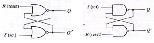
SR latch with NOR Gate
SR Latch has two useful states:
•Set state, when output Q=1 and Q'=0.
•Reset state, when output Q=0 and Q'=1.
These states to can be used to store 1-bit information.Output Qand Q' are usually complement of each other.
•Undefined state, when Q=0 and Q'=0, occurred when both inputs Rand Sare equal to 1 at the same time.
•Under normal conditions, both inputs of the latch (Rand S) remain at 0 unless the state has to be changed.
•To let latch in the set state, Smust be 1
•To let latch in the reset state, Rmust be 1
•The inputs Sand Rmust go back to 0 before any other changes to avoidthe occurrence of the undefined state.
•The latch go to the set state or reset state and stay there even after both inputs return to 0.