Examine the operation of the rs latch

Assignment Help Electrical Engineering
Reference no: EM13841769

The objectives of this experiment are to:

1. Examine the operation of the RS latch.

2. Examine the operation of the D-type flip flop.

3. Examine the operation of the JK flip flop.

Introduction A flip flop is an essential building block of many important and useful circuits, such as counters, shift registers, and memories.

Basically, a flip flop stores a zero or a one. One or more inputs are provided to change the state of the flip flop. In this experiment we will examine the operation of several common flip flops.

Procedure 1. Load the circuit E6A-1.MS7, shown in Figure 6A.1

1766_1.png


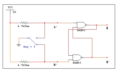
Figure 6A.1: RS latch

Attach logic indicators and simulate the circuit. Which indicator is on?

2. Press ‘T' several times. What happens at the Q and Q' outputs?

3. In the real world, the SPDT switch suffers from mechanical contact bounce, which in turn generates hundreds or even thousands of edges before settling. The RS latch debounces the switch, providing one clean edge on its output for each toggling of the input. This edge can be used to provide a single clock pulse to a flip flop, counter, or shift register. MultiSim contains several built-in RS latches in the Miscellaneous Digital parts bin.

Figure 6A.2 shows one example.

746_2.png

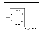
Figure 6A.2: Built-in RS latch

Add the SPDT switch to the inputs with the proper pullups and verify that the built-in RS latch works the same as the circuit in Figure 6A.1.

4. Load the circuit E6A-2.MS7, shown in Figure 6A.3, which uses the RS latch as the clockpulse circuit for a D-type flip flop. The data input to the flip flop is controlled by the D switch.

167_4.png

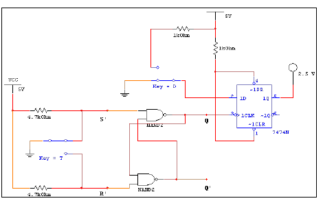
Figure 6A.3: Type-D flip flop

5. Determine what edge the D flip flop responds to (positive or negative).

6. Load the circuit E6A-3.MS7, shown in Figure 6A.4. The D flip flop has its Q' output wired back to the D input. This enables a special mode called toggle, where the state of the output alternates between zero and one every two clock cycles. Verify this by pressing ‘T' ten times.
How many times does the logic indicator flash?

99_6.png


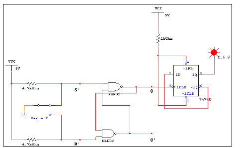
Figure 6A.4: D flip flop wired for toggle mode

7. Load the circuit E6A-4.MS7, shown in Figure 6A.5.

972_7.png

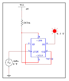
Figure 6A.5: Divide-by-two circuit

Verify (using the oscilloscope or logic analyzer) that the frequency of the waveform at the Q output is 500 Hz.

8. Add a second D flip flop (wired for toggle). The Q output of the first flip flop connects to the clock input of the second. What is the frequency at the second Q output?

9. Load the circuit E6A-5.MS7, shown in Figure 6A.6. Now the asynchronous preset and clear inputs are used. The upper input (connected to the P switch) is the Preset input, which causes Q to go high, regardless of the clock state, whenever Preset is low. The lower input is the activelow Clear input, which forces Q low when active. Verify the operation of the Preset and Clear inputs by toggling ‘P' and ‘C' during simulation.

535_9.png


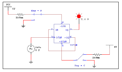
Figure 6A.6: D flip flop with asynchronous inputs

10. Load the circuit E6A-6.MS7, shown in Figure 6A.7.

1156_10.png

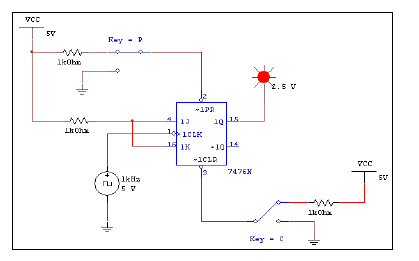
Figure 6A.7: JK flip flop wired for toggle mode

11. With the J and K inputs tied high, the output of the JK flip flop will toggle to the opposite state upon each negative edge of the clock. Verify that the JK flip flop is negative-edge triggered.

12. Verify that the Preset and Clear inputs are active low (using ‘P' and ‘C').

13. The truth table for the JK flip flop is shown in Table 6A.1. Verify the four modes of
operation.

2098_13.png


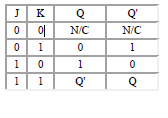
Table 6A.1: Truth table for the JK flip flop

When J and K are both low, the outputs do not change state when the flip flop is clocked. When J is low and K is high, Q goes low after the next clock pulse. This mode is called clear. When J is high and K is low, Q is set after the next clock pulse. Toggle mode is selected when J and K are both high. "What is the difference between a synchronous input (D, J, or K) and an nchronousinput(PR or CLR)?"
Discussion
While reviewing your data and results, provide detailed answers to each of the following:
1. How does the built-in RS latch in the Miscellaneous Digital parts bin differ from the NAND gate circuit in E6A-1.MS7?

2. Do the type-D and JK flip flops respond to the same clock edge?

3. Explain how toggle mode is the same as division by two.

4. What is the difference between a synchronous input (D, J, or K) and

Attachment:- m5_multisim_lab.zip

Reference no: EM13841769

Questions Cloud

Product of the grid od approach to management : Which of the following is a product of the Grid OD approach to management?
Calculate the beta of a portfolio : What is the beta of an asset with an expected return of 16%, if the risk-free rate of interest is 6% and the expected market portfolio risk premium is 6%? Accurate to two decimal places.
What is fraud : What is fraud. What is the difference between fraud and abuse. According to the fraud profile in the text, who are the perpetrators of fraud, and how do their characteristics affect fraud losses
Analyze the sexual harassment issues presented in scenario : Analyze the sexual harassment issues presented in scenario. Analyze ech of the elements of this case: the applicable defenses and the basis for the court's ruling.
Examine the operation of the rs latch : Examine the operation of the D-type flip flop
Research the recent google/apple/ebay/intuit : Research the recent GOOGLE/APPLE/EBAY/INTUIT AntiTrust Violations Case and write 1-2 paragraphs (typed) analyzing the issue and outcome.
Discuss careers in forensic accounting : There are many exciting careers in forensic accounting. Here are just a few of the specializations from which you should choose one
What do you think with strong credit explanation letters : Home mortgage loans to buyers with low credit scores of 500-580 what do you think with strong credit explanation letters
Designing an organizational structure : There are many elements to consider when designing an organizational structure. Let's start by each of picking one of the six key elements and discussing why that element is important to the overall success of the design. Please cite your sources.

Reviews

Write a Review

Electrical Engineering Questions & Answers

  Find what is the real power applied to the motor in watt

A motor with efficiency of 76% supplies 20 hp to a load. it's power factor is 0.6 (lagging). A voltage of 440 VAC (RMS), 60 hz is applied to the motor. a) what is the real power applied to the motor in Watt

  Calculate the resistor values in the designs for scaling

Frequently, the output of transducers are much smaller than what an A/D converter expects on its input. That would require an amplifier to match it. Sometimes the output does not start at 0V. Usually the minimum reference input voltage of an A/D

  What is the minimal sum of product form

What is the minimal sum of product form for the following switching function

  Find a state table with a minimum number of states

Design a sequential circuit which adds two to a binary number in the range 0000 - 1001. The input and output should be serial with the least significant bit first. Find a state table with a minimum number of states.

  Design a 4 bit register with 4 different kinds of flip flops

design a 4 bit register with 4 different kinds of flip flops, that has at least 12 different functions. list clearly the functions. Do something creative, and say exactly your innovation. at least one flip flop should have some input besides a mul..

  The output response for a system is given as vot a1 -

the output response for a system is given as vot a1 - e-at sinat. is this a proper representation for an output

  Determine mechanical power supplied to the load

When the motor runs at 1710 rpm, the line currentdrawn from the supply is 78 A at 0.85 PF lagging. Given that,stator iron loss is 2kW, windage and friction losses are 1.2kW andresistance between two stator terminals = 0.4W

  Analog signals in telecommunications and the digital

Supporting Activities: Introduction to Modems

  Calculate load voltage v2 and transformer voltage regulation

In a two-winding transformer N1 = 2000 and N2 = 500 and the supply voltage V1 = 1200 V. The transformer has winding resistances R1 = 2.0ohm and R2 = 0.125ohm , and leakage reactances X1 = 8.0 and X2 = 0.5ohm

  Give detailed explanations for both telecommunication system

In telecommunication systems, Time-Division Multiplexing and Frequency -Division Multiplexing are used. Give detailed explanations for both systems and give succinct examples for each of them.

  Find out the minimum signal to noise ratio

Determine the minimum signal to noise ratio (s/n) in dB required in each communication channel to achieve a data rate of 270 kbps?

  What is total input current and power factor of transformer

Two single phase transformers are connected in parallel with the following parameters. Transformer A, rated at 60 kVA Rc=250 k Ohm Req=25 Ohm Xm=45 k Ohm Xeq=150 Ohm

Free Assignment Quote

Assured A++ Grade

Get guaranteed satisfaction & time on delivery in every assignment order you paid with us! We ensure premium quality solution document along with free turntin report!

All rights reserved! Copyrights ©2019-2020 ExpertsMind IT Educational Pvt Ltd