Reference no: EM132845007
ELEC 20004.1 Digital Communication - Middle East College
Learning Outcome 1: Differentiate the types of pulse modulation techniques implemented in communication systems;
Learning Outcome 2: Critically evaluate the baseband demodulation and detection techniques;
Learning Outcome 3: Critically evaluate digital modulation techniques including multi-level digital modulation
Task 1 - Submit a work proposal for this assignment on or before 05/04/2021 (23:59) which must include:
Understanding of deliverables - a detail description of deliverables.
General overview of proposed plan - initial understanding of solution to task2.
Timeline for completion of the given tasks.
The work proposal must be submitted in a word file through the link available in Moodle.
Task 2
Q1.
a) A waveform x(t) = [15 cos (2500t + Π/4) x 25 cos(1500t + Π/8)] is to be uniformly sampled for digital transmission.
1. What is the maximum allowable time interval between sample values that will ensure perfect signal reproduction?
2. If we reproduce 3 hours of this waveform, how many sample values need to be stored.
3. Sketch the frequency spectrum of sampled waveform.
4. Specify the minimum cut off frequency of the ideal reconstruction filter so as to recover x(t) from its sampled signal
b) Suppose you want to transmit the 8 bit message [x x x x x x x x] by Pulse-code Modulation (PCM). Using clearly labeled diagrams, show the encoding the bit sequence using the following PCM waveform types:
i. Unipolar RZ signal
ii. NRZ-AMI
iii. Bi - φ - L
iv. Delay modulation
Q2.
a) Design a circuit using 741 op amp IC and 555 timer IC, to generate both Pulse Width and Pulse Position modulated signals. Perform the required calculations to obtain the width of the PPM signal as 200µs. Draw the clear circuit diagram and calculate the values of resistors and capacitors used.
b) Simulate the circuit designed in part (a) using appropriate simulation tools(Multisim or Tinkercad) and obtain the output. The answer should include details such as aim, brief procedure, screenshot of simulation circuit along with resultant waveforms and calculations of the practical time-period obtained for PPM output.
c) Plot graphs with clear labels and scales for message, carrier and output signal (PWM and PPM). Also discuss your inference and reflection on the results obtained.
Q3.
a) The highest frequency of a signal is 25kHz(Sinusoidal). If it is sampled at the following sampling interval, can you able to recover the original waveform at the receiver? Prove each case with the help of clearly labelled graphs(Plot the graphs with respect to time)
The waveform is sampled at 20μs interval
The waveform is sampled at 40μs interval
Write a reflection on the effect of different sampling time Ts in the part I and ii.
b) An 10 bits single channel PCM system gives an output of 102 kilo bit per second(kbps). Calculate:
The sampling frequency of the system.
The highest possible modulating frequency of the system.
The bit duration of the system.
The Bandwidth of the system.
c) A channel is providing a S/N ratio of 65dB. When the bandwidth of signal is 22 KHz, the value of Eb/N0 is found to be 40dB. If same channel is used with same signal bandwidth but with a different data rate. It is observed that the new Eb/N0 is reduced by 40% of its initial value. Calculate the new value of Eb/N0 and data rate.
Q4.
Delta modulation suffers from several types of noises; one of these noises is called Slope Overload Noise. Explain this type of noise in delta modulation including your explanation for the reason(s) of this type of noise and how can it be avoided?
A continuous time signal is given (in volt) by:
m(t) = 10-4 cos(2Π105t)
It is required to approximate m(t) by using delta modulation. What is the minimum step size ? of the delta modulation to avoid slope overload noise? Assume the sampling frequency is 42 kHz.
Amplitude Shift Keying (ASK) is a type of Digital Modulation technique which represents the binary data in the form of variations in the amplitude of a signal.
Design an ASK modulation circuit and simulate the design using multisim or tinkercad (attach the screenshot along with your answer) and plot graphs with clear labels and scales for message, carrier and output ASK signal. Given than message signal m(t) is 3Vp, 500Hz and carrier signal is 4Vp,2.5kHz
Note: Plot the graphs in a graph paper by hand and attach the scanned copy to the assignment
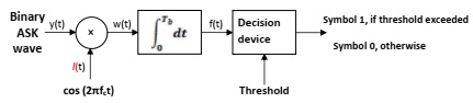
A block diagram of binary ASK demodulation is shown in the figure 1. Explain the operation of the receiver and the demodulation process. Also write the mathematical expressions for the signals y(t), w(t) and f(t).
Attachment:- Digital Communication.rar