Draw out the logic diagram of the multiplier

Assignment Help Electrical Engineering
Reference no: EM131932790

Lab 2 Procedures

Part I - Design a Multiplier

In the part of the lab, you are required to design a multiplier, which does the multiplication of a 3-bit number B(2:0) by a 4-bit number A(3:0).

The multiplication process can be illustrated as follows:

237_Untitled.png


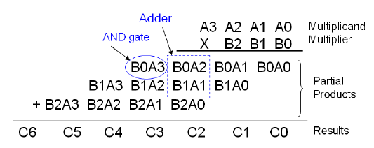
You are required to use half adders, full adders and AND gates to implement this multiplier.


  1. Design: draw out the logic diagram of the multiplier (e.g. see the logic diagram of a 2-bit and 2-bit multiplier illustrated in the Pre-lab and Background Information). Remember, you may only use half adders, full adders and AND gates. You will need to include this logic diagram in your lab report.
  2. Create a new design file "YourFirstNameLastNameLab2Part1" under your default design directory/folder.  In this design file, draw the circuit you have designed from step 1. You may use SPDT switches to provide the multiplicand and multiplier inputs. You may also use LED arrays to demonstrate your resulting binary number of the multiplier (each LED can be used for a single bit in the multiplier result).
  3. Run simulations to test your design. You should test a few possible pairs of the numbers A and B, e.g. multiply the decimal equivalents: 8x2, 11x3, etc. You should verify that the results generated (as indicated in the LED lights if you choose to use the LED lights to demonstrate your multiplication results) are correct for each of the number pairs. Capture a screenshot for each of the A & B number pairs you tested and include an explanation on how you can conclude that your circuit is functioning correctly.
  4. Once you have verified your design logically in step 3, use your multiplier to conduct the following multiplications, use a table to list your inputs and expected outputs. Capture a screen shot for each of the following multiplications and include an explanation on how you verify that your circuit does the multiplications correctly for the following cases.
    1. 5x3
    2. 15x5
    3. 9x7
    4. 15x7


Part II - Design a Synchronous Counter


Design a synchronous counter to produce the following binary sequence. Use J-K flip-flops and other gates necessary:

1 - 4 - 3 - 5 - 7 - 6 - 2 - 1 - 4 - .......

  1. Design: draft the specification for the counter including the inputs and outputs. Construct state tables based on your specification, and use the K-map if necessary to optimize your functions for the outputs. Include the specification, input/output definitions, state tables, and the K-maps in your lab report.
  2. Create a new design file "YourFirstNameLastNameLab2Part2" under your default design directory/folder.  In this design file, draw the circuit you have designed from step 1. You may use SPDT switches to provide control inputs. You may use LED arrays to show your binary sequence or use a 7-segment display to display the binary sequence in a human readable manner.
  3. Run simulations to test your design. You should verify that the counter you design generates the correct sequence. Capture a series of screenshots to demonstrate the correct sequence generated by your counter and include a short explanation on how you can conclude that your circuit is functioning correctly.


Part III - Design a Shift Register


A Shift Register is a series of flip-flops connected so that data can be transferred to a neighbor each time the clock pulse is active. These shift registers can be constructed using D or J-K flip-flops.

A shift register counter is a shift register with the serial output connected back to the serial input to produce special sequences. Two of the most common shift register counters are the Johnson Counter [Twisted Ring Counter] and the Ring Counter [Overbeck Counter].

  1. Conduct research on what Ring Counter and Johnson Counter are and what their expected functions are. Include your research results in your lab report.
  2. Build a 5-bit Ring Counter using J-K flop-flops, and again using D flip-flops. Include the state tables and confirm that each produces five states.
  3. Build a 5-stage Johnson Counter using J-K flip-flops, and again using D flip-flops. Include the state tables and confirm that each produces ten states.
  4. Create a new design file "YourFirstNameLastNameLab2Part3" under your default design directory/folder.  In this design file, draw the circuit for all the four counters you have designed from step 1 and step 2. Apply the same clock source to all the four counters and use different LED arrays to demonstrate the outputs of each counter.
  5. Run simulations to test your design. You run through all the possible states for your Ring Counters as well as your Johnson Counters. Capture a series of screenshots to show all the states of your counters in the correct sequence and include an explanation on how you can conclude that your counters are all functioning correctly.

Reference no: EM131932790

Questions Cloud

Does the us have a responsibility to protect the people : Write a minimum five-page paper assessing the economic, military and humanitarian conditions in the developing world that have been affected.
Summarize key elements of the research study : In this section of your final project, you will summarize key elements of the research study and analyze the population impacted by the health issue.
Effective duration measures-macaulay duration measures : Effective duration measures. Modified duration measures. MacAulay duration measures
What is the probability of correctly guessing all 6 values : The current jackpot is 730 million money units. What is the probability of correctly guessing all 6 values with just one ticket?
Draw out the logic diagram of the multiplier : Design: draw out the logic diagram of the multiplier (e.g. see the logic diagram of a 2-bit and 2-bit multiplier illustrated in the Pre-lab and Background Information). Remember, you may only use half adders, full adders and AND gates. You will need ..
The cost of capital-weighted average cost of capital : What is the firm's weighted average cost of capital (WACC1) if it uses retained earnings as its source of common equity?
Evaluating financial performance of motor sports association : You are required to prepare a report, evaluating the financial performance of Motor Sports Association UK, over the four-year period ending 31st December 2016.
Percentage of grand jury members who were immigrants : Construct a? 99% confidence interval for the percentage of grand jury members who were immigrants.
Different securities carrying the same amount of risk : William and Kate invest in two different securities carrying the same amount of risk.

Reviews

Write a Review

Electrical Engineering Questions & Answers

  Calculate the turn ratio of the output transformer

Audio amplifiers use transformer coupling between the final amplifier stage and a speaker to match impedances and in order to avoid having DC current of the final stage flow through the speaker coil. We wish to connect an 8 Ω speaker to an 8000 Ω ..

  Power system analysis and design

Power System Analysis and Design - Electrical Design of HV Power Transmission Lines and describe in 500 words the impact of power transmission line on society

  What is the frequency

The output response for a system is given as Vo(t) = A(1-e^-at)sin(ωt). Is this a proper representation for an output response given that it contains a sinusoidal term? Fully explain your answer.

  What fraction of the widths of the strip should be added

A 78oham lossless planar line was designed but did not meet a requirement. What fraction of the widths of the strip should be added or removed to get the characteristic impedance of 75oham

  What is the output snr of matched filter

if Eb the energy per bit of a binary digital signal, is 10^-5 watt-sec and the one sided power spectral density of the white noise ,N0= 10^-6w/hz then what is the o/p SNR of matched filter.

  What are the key decisions that have to be made

Compare Wi-Fi and high-speed cellular systems for accessing the Internet. What are the advantages and disadvantages of each?

  What is the peak instantaneous power of the laser

(a) What is the peak instantaneous power of the laser (b) If only 100 pulses can be generated per second, what is the average power output of the laser

  Make a transfer function with numerator and denominator

Make a transfer function with numerator p(s) and denominator q(s)that will separate only the 3cos(4t) portion from the noise corrupted function: u(t) = sin(25t) + 3cos(4t) + n(t) wheren(t) is random noise. The degree of the polynomial on the denom..

  What is the maximum number of consecutive bits

What is the maximum number of consecutive bits that are in error for a transmission through this channel if the data rate is 10Kbps? If the data rate is 11 Mbps?

  Find flux density and energy stored in air gap as function

A certain iron core has an air gap with an effective area of 2 cm×3 cm and a length lg. The applied magne to motive force is 1000 A· turns, and the reluctance of the iron is negligible. Find the flux density and the energy stored in the air gap a..

  Compute the power

If the current through and voltage across an element are I = 8 sin(ωt + 40°) and v = 48 sin(ωt + 40°), respectively, compute the power by I2R, (VmIm/2) cos θ, and VI cos θ, and compare answers.

  Calculate is and the current i for v for a pn junction

Calculate Is and the current I for V = 700 mV for a pn junction for which Na = 1017 / cm³, Nd = 1016 / cm³, A = 200 µm², ni = 1.5 x 10^10 / cm³, Lp = 5 µm, Ln = 10 µm, Dp = 10 cm² / s, and Dn = 18 cm² / s

Free Assignment Quote

Assured A++ Grade

Get guaranteed satisfaction & time on delivery in every assignment order you paid with us! We ensure premium quality solution document along with free turntin report!

All rights reserved! Copyrights ©2019-2020 ExpertsMind IT Educational Pvt Ltd