Reference no: EM131216124
Introduction
This experiment has been designed to give experience in practical design and performance measurement of bipolar junction transistor (BJT) amplifiers, principally in hardware implementations.
Section 1 deals with the design of a single-stage series feedback amplifier where you are asked to work out its operating conditions and confirm - or otherwise - that they are correct, and then assess its actual performance as an amplifier. This can be done both in a Multisim simulation and in the hardware implementation. The design is later modified in a way that significantly increases its input resistance - and hence loading on any previous stage - by using a technique called bootstrapping.
Section 2 adds a second stage of amplification; the aim here is to investigate distortion and any effects of interstage loading on the overall gain. Alternative two-stage designs can also be considered.
Section 3 lists useful sources of additional information and Section 4 covers assessment and reports.
The principal reference is: Chap. 6, Electronic Devices, 5th ed., Floyd, T. L. (Pearson/Prentice Hall).
1. Bootstrapped bias
1.1- Design of series feedback amplifier
The experimental circuits are constructed as needed on plug-in breadboards - see Appendix A for details. The BJT devices used are of type BC184 (and its pnp complement BC214). A manufacturer's data sheet for BC184 is given in Appendix C.
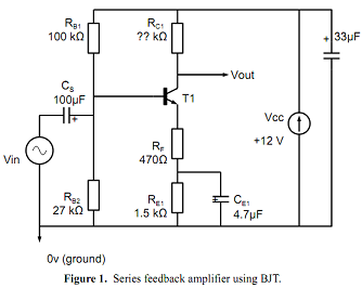
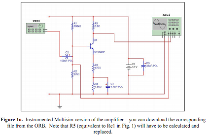
The partially designed and constructed series feedback circuit is shown in Figure 1. A Multisim implementation of the circuit (see Fig. 1a) is available for download from the ORB, but note that the value for the collector resistor is set at 0Ω which is not correct!
Design, calculation and simulation
To save time in the laboratory, it is best to do the following calculations in advance of the experimental work.
(a) Calculate a value for RC1 to achieve a mid-band voltage gain of approximately -10.
(b) Determine the bias conditions for the transistor (i.e. collector voltage, base voltage, emitter voltage, collector current and emitter current).
(c) Check with your calculated value of RC1 that the collector voltage can swing both above and below its bias level by approximately equal amounts. Why is this desirable feature?
(d) Confirm that for the component values shown in Figure 1 the 3-dB break frequency at low frequency is determined mainly by CE1, RE1 and RF. Hence calculate the low-frequency breakpoint.
(e) Calculate the mid-band input resistance of the amplifier assuming that both CS and CE1 have negligible reactance. If transistor base-collector current gain β increases from 150 to 300 what percentage change in input resistance occurs?
(f) What is the ultimate rate of attenuation with frequency (dB/octave) at very low frequency?
(g) Figure 1 includes a 33µF capacitor (not shown in other circuits) connected across the power supply. It can be seen at the top right of the photograph in Appendix A, but does not affect the design aspects of the system. What is the essential function it performs, which is the same for any piece of electronic circuitry?
Measurements
General advice on measurements- AC signals can be measured on the oscilloscope (use averaging capture mode) or using an analogue millivoltmeter - the latter is sometimes useful as results can be expressed directly in decibels. However, you should always monitor the signal waveform at the same time to ensure that is it not being clipped because of limited dynamic range. Voltmeter readings from a distorted waveform are meaningless!
If you are measuring a frequency response, the results should normally be plotted on a graph with gain in dB versus frequency, and the frequency axis should be logarithmic: for a range of 10 Hz to 1 MHz you will need to set the axis to 5 cycles (corresponding to 10 Hz, 100 Hz, 1 kHz, 10 kHz, 100 kHz and 1 MHz). It is strongly recommended to do a quick plot of results as you take them, ideally by immediate entry into a spreadsheet. To get equally-spaced points on the graph, the frequencies at which measurements are taken should have a roughly constant ratio (not increment), for example 10, 15, 22, 33, 47, 68, 100, 150... and so on (ratio ≈ 1.5). This sequence of numbers should be familiar from another context. Where the response is changing rapidly, near -3 dB points for example, the measurement point density should increase. A highly-recommended and extremely powerful graph plotting application is Gnuplot, available free for most operating systems; for more information, see:
https://www.gnuplot.info/
Waveform images can be captured to USB memory stick from the oscilloscopes: if you do this, to get a noise-free trace remember to set the oscilloscope to 'Average' mode (via the Acquire menu button).
(a) Construct the circuit on the breadboard, copying the layout in Appendix A if you have not done this before. The original used for the photograph will be available for inspection in the laboratory. The layout copies the actual circuit diagram quite closely. Be very careful with the transistor connections which can vary: the most common version for the BC184 type is 'bce', left to right looking onto the leads with the curved part of the transistor upwards. This is different from Appendix C.
(b) Measure and plot the input-output amplitude response over a frequency range of 10 Hz to 1 MHz using either an AC millivoltmeter or a digital oscilloscope, and obtain a gain reading in decibels. Identify the mid-band gain and the low-frequency breakpoint and compare them against the predicted values. Is the gain accurately defined by a resistor ratio? If not, what might account for a small difference from -10?
(c) Measure the input resistance of the amplifier at 1 kHz and compare it to the theoretical prediction - if you are not sure of the very easy way to do the measurement, ask a demonstrator. What is the dominant factor that determines the input resistance?
(d) Investigate the overload performance by progressively increasing the input signal amplitude until the output waveform is severely distorted. Some very subtle effects can be seen here, which you should record and explain, and certainly discuss with the lab staff.
(e) Measure the upper 3dB cutoff frequency of the amplifier. This can be done either by extending the measurement range of (b) to (say) 10 MHz, but there are two quick ways to do it. The first is to set the output signal amplitude at some convenient level, say 2 V pk-pk, for an input at 1 kHz, then increase the signal generator output frequency until the output voltage drops to the level equivalent to -3dB. The second method measures rise (or fall) time in response to a square-wave input signal. Then it can be shown that, in simple cases like this:
Bandwidth × Risetime ≈ 0.35
(f) Use the oscilloscope to examine and record the amplifier output for very low frequency square-wave inputs (1 - 10 Hz). Explain what you see, but note that it is essential for the oscilloscope input coupling to be set to DC for this to work properly.
Appendix B gives more information on time-domain (risetime/falltime) measurements using the oscilloscope.
1.2- Bootstrap bias circuit
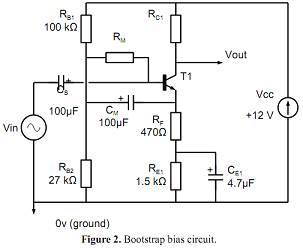
In this experiment you are required to modify the amplifier circuit of Figure 1 to incorporate bootstrap biasing as shown in Figure 2. If you are not certain what 'bootstrapping' means, ask a demonstrator, but in summary it increases the apparent value of the resistor RM for AC signals so reducing the load it imposes on the input signal1.
Assuming that the reactance of all capacitors is negligible, calculate the mid-band voltage gain between the input and an output taken at the transistor emitter. Then, taking bootstrapping into account, calculate RM so that its contribution to the mid-frequency input resistance is approximately 100 k?.
A suggested value for CM is 100 µF - not critical.
Measurements
(a) Add RM and CM to the circuit, noting the correct polarity for CM. Re-measure the bias conditions of the amplifier and confirm that the introduction of RM has not had a significant effect.
(b) Measure both mid-band input resistance and voltage gain and compare against your earlier measurements and calculation. Account theoretically for any change in input resistance.
(c) Note that the frequency response at very low frequencies may show an undesirable resonance peak. Justify your measured results by analysing the low frequency transfer function and show that at low frequency the input impedance can appear partially inductive, which can resonate with the input coupling capacitor. Using Multisim, investigate the low frequency response of the amplifier for a range of CS from 0.1 µF to 100 µF. A very low frequency square-wave input may give useful insights here.
2. Multi-stage amplifier
2.1- AC coupled, cascaded npn transistor stages
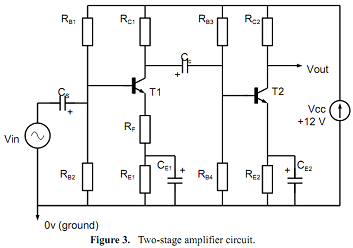
Construct the multi-stage amplifier shown in Figure 3 by adding a 'copy' of the circuit in Figure 1, but note that the second stage has no AC emitter degeneration (i.e. RF2 = 0 Ω) so you will need to choose an appropriate value for RE2. Cc should be connected to the collector of the first transistor.
Measurements
A problem- When doing the following measurements, as noted previously, you should monitor the output signal on the oscilloscope to ensure that it is not distorted. Because the overall gain of the two stages is so large it will be impossible to reduce the signal generator output sufficiently to avoid output 'clipping'. The solution is to insert an attenuator at the input; a potential divider using 1000 ohm and 10 ohm resistors is recommended (or 990 (=890+100) and 10 ohms if you want a very precise factor of 100!). Measure the signal generator voltage to the amplifier at the input to the attenuator, and then take its attenuation factor into account in the gain calculation - the signal at the amplifier input itself will be too small to measure easily with the standard lab instruments.
With the two amplifiers connected together:
(a) Measure the mid-band gain from input to the output of the first stage and compare this with the gain measured in Section 1.1.
(b) Why is the overall gain not equal to the product of the individual stage gains when they are measured with the two stages disconnected from each other?
(c) Measure the mid-band gain from input to the output of the second stage. Compare your results with the theoretical gain incorporating relevant information from the bias conditions.
(d) Measure the overall frequency response over the range 10 Hz to 1 MHz and relate this to the gains determined above.
(e) Find the upper 3dB cutoff frequency of the 2-stage amplifier.
(f) A configuration like this would not be used in any practical application, and both stages would typically have feedback. Modify the second stage to do this: the easiest way is simply to copy the emitter circuitry of stage 1. Make the individual stage gains both nominally 10, and measure overall performance.
2.2- Direct coupled npn-pnp stages
This circuit (Figure 4) uses complementary npn and pnp transistors.
(a) Design and build the second stage of the two-stage amplifier as shown in Figure 4, a useful configuration that reduces the number of biasing components and also omits the coupling capacitor. The design reuses the idea from 2.1(f) of both stages having series feedback (i.e. insert RF2/CE2 in the emitter connection of T2).
Calculate RE2 + RF2 to bias T2 at the same collector current as the common-emitter amplifier in Section 1.1 and make the nominal gain of the second stage also 10.
You should find that the overall gain of this version of the 2-stage design is more closely related to the gains of the individual stages. Explain why.
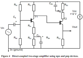
A suitable pnp transistor for T2 is BC214 (complement to BC184). Remember to include a decoupling capacitor across the power supply lines.
Attachment:- Assignment.rar