Contamination and briefly describe physical characteristics

Assignment Help Electrical Engineering
Reference no: EM132122744

1. (a) Name the three major groups of contamination and briefly describe their physical characteristics.

(b) Where do the above contamination types come from? Give one example of each.

2. Name two processes metrics which would be worsened by poor cleanroom practices in a semiconductor cleanroom. Describe briefly what is meant by each term.

3. (a) What sizes of particles would cause problems for the following processes:

- 5 μm bipolar

- 4.5 μm NMOS

- 1.1 μm CMOS

- 0.9 μm BICMOS

- 0.3 μm CMOS?

(c) What effect is illustrated by the above?

(d) What additional particle related issue affects smaller feature size processes?

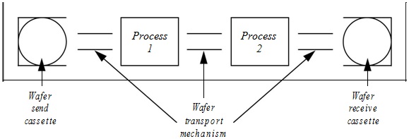
4. FIGURE 1 shows a system which is to be assessed for particles. The maximum specification limit on the system is +100 particles of >0.5 μm.

(a) A CWC is run by processing a test wafer through the entire sequence (process module 1 and module 2) and it reveals that 350 particles of >0.5 μm have been added. Comment on this finding.

(b) A second CWC is run with the wafer being processed only through module 1 and it reveals that 334 particles of >0.5 μm have been added. Comment on this finding.

(c) A third CWC is run with the wafer being processed through module 2 and it reveals that 328 particles of >0.5 μm have been added. Comment on this finding.

(d) Suggest where the particles may be coming from and suggest ways to isolate the sources of particles.
113_Top view.jpg

FIG. 1

5. The approximate number, N, of square chips of area A that can be formed on a wafer of diameter D is given by the equation:

N ≈ π/4A.(D - √A)2

A VLSI chip is to be fabricated on a 300 mm wafer and uses 6 lithography processes. It is reckoned that on average there will be 2 defects per wafer for each lithographic process. Assume the defects fall on different chips.

Calculate the cumulative percentage yield of the lithography processes if the chip has an area of:

(a) 0.5 cm2

(b) 1 cm2

(c) 2 cm2

(d) 4 cm2.

Comment on the results.

Verified Expert

In this task we have covered groups of contamination,cumulative percentage yield of the lithography processes as well as operation of a range of semiconductor

Reference no: EM132122744

Questions Cloud

Identify common inherent risk factors : Identify common inherent risk factors that companies involved in the entertainment industry pose for their independent auditors.
Represent the height of first graders in a class : Let x represent the height of first graders in a class. This would be considered what type of variable:
How many orders does the company place per year : Assume that it is Monday morning before the store opens, and a shipment of suits has just arrived. How many orders does the company place per year?
Share two new aspects of leadership : Share two new aspects of leadership that you learned by analyzing application of theory.
Contamination and briefly describe physical characteristics : Calculate the cumulative percentage yield of the lithography processes if the chip has an area - What additional particle related issue affects smaller feature
New medication for lung cancer : A medical researcher is interested in determining whether a new medication for lung cancer is effective in a group of patients with early
Define the parameter of interest : (a) Define the parameter of interest and state null and research hypotheses. (b) Determine the characteristics of the comparison distribution.
How do institutions-resources affect multinational strategy : How do institutions and resources affect multinational strategy, structure, and learning?
Tabulate the minimum sample size needed : The half-width B desired could be anywhere from 2 to 7. Tabulate the minimum sample size needed for the given ranges of sigma and B.

Reviews

urv2122744

10/27/2018 4:58:12 AM

I got the best solution in an affordable prize. I strongly recommend ExpertsMind to all students seeking to get help in their assignments. It is the best way to receive excellent quality work without making any effort. As soon as you start working with the team, you realize you will never want to leave them. I must say you guys are done an amazing job.

urv2122744

10/27/2018 4:56:34 AM

4. Critically compare different process methods used to achieve the same state in an overall structure. Practical and Professional Skills 5. Demonstrate an awareness of current developments in semiconductor fabrication. 6. Detail the need for cleanroom practise in the semiconductor industry. Key Transferable Skills 7. Apply numerical skills to a variety of problems relating to semiconductor structure and fabrication. PASS Learning outcomes are satisfied as evidenced by substantially correct understanding of the requirements of cleanroom practice. MERIT Criteria in excess of the pass grade. The transfer of competence gained in one situation to related but unfamiliar circumstances. DISTINCTION Criteria in excess of the merit grade. The ability to integrate knowledge from two or more topic areas to solve a more complex problem.

urv2122744

10/27/2018 4:55:59 AM

Assessment Criteria This assignment relates to cleanroom practice involved in the manufacture of semiconductor devices.. The assignment forms Element 3 of the module’s assessment criteria that covers in part Learning Outcomes 6 and 7 as indicated below. MODULE LEARNING OUTCOMES Knowledge and Understanding 1. Demonstrate an understanding of the structure, properties and operation of a range of semiconductor devices. 2. Demonstrate knowledge of the processes and equipment involved in the manufacture of a range of semiconductor devices. Cognitive and Intellectual Skills 3. Select the appropriate processing steps required to realise a given semiconductor structure or device.

Write a Review

Electrical Engineering Questions & Answers

  Lithium ion battery technology

The paper includes Lithium ion battery technology with its advantages and disadvantages. The paper discusses about the Lithium air battery in which detailed reactions of Lithium with air including nonaqueous as well as aqueous are given.

  Power transformers and tariffs

Construction of different types of power transformer, significant energy savings

  Paper on orthogonal frequency-division multiplexing

This document is shown a paper on Orthogonal frequency-division multiplexing with advantages, disadvantages and uses.

  Function of the hmi in a scada system

This assignment contains electronics engineering questions like State the commonly found components of a SCADA (Supervisory control and data acquisition) system. and decribe the function of the HMI in a SCADA system.

  Resultant waveform of the odd harmonic series

Prepare an Excel graph showing the individual components and summated resultant waveform of the odd harmonic series resulting in an approximate square wave.

  Explain scada system

Explain the function of the HMI in a SCADA system.

  Design a 2-digit 24 second shot-clock

Design a 2-digit 24 second "shot-clock" countdown timer with pushbutton controller.

  Model a discrete-time system

To understand di erent signal models To be able to model a discrete-time system and design simple signal processing algorithms.

  Draw a relay construction diagram

Draw a relay construction diagram and briefly explain the operation of a relay.

  Frequency division multiplexing

Write a short technical report on Frequency Division Multiplexing

  Impact of electron energy

Briefly discuss the impact of electron energy, electron current and target on the Bremsstrahlung generated.

  Traffic light controller

The schematic of the traffic light controller

Free Assignment Quote

Assured A++ Grade

Get guaranteed satisfaction & time on delivery in every assignment order you paid with us! We ensure premium quality solution document along with free turntin report!

All rights reserved! Copyrights ©2019-2020 ExpertsMind IT Educational Pvt Ltd