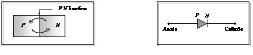
When a P-type semiconductor is suitably joined to an N-type semiconductor, then resulting arrangement is called P-N junction or P-N junction diode
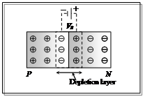
Depletion region: On account of difference in concentration of charge carrier in the two sections of P-N junction, the electrons from N-region diffuse through the junction into P-region and the hole from P region diffuse into N-region.
Due to diffusion, neutrality of both N and P-type semiconductor is disturbed, a layer of negative charged ions appear near the junction in the P-crystal and a layer of positive ions appears near the junction in N-crystal. This layer is called depletion layer
|
(i) The thickness of depletion layer is 1 micron = 10-6 m.
(ii) Width of depletion layer ∝ 1/Dopping
(iii) Depletion is directly proportional to temperature.
(iv) he P-N junction diode is equivalent to capacitor in which the depletion layer acts as a dielectric.
|
|
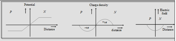
Potential barrier: The potential difference created across the P-N junction due to the diffusion of electron and holes is called potential barrier.
For Ge vB =0.3v and for silicon vB = 0.7v
On the average the potential barrier in P-N junction is ~ 0.5 V and the width of depletion region ~ 10-6.
So the barrier electric field E = V/d =0.5/10-6 =5 * 105 v/m
Some important graphs:
Diffusion and drift current: Because of concentration difference holes/electron try to diffuse from their side to other side. Only these holes/electrons cross the junction, having high kinetic energy. This diffusion results is an electric current from the P-side to the N-side known as diffusion current (idf)
As electron hole pair (because of thermal collisions) is continuously created in the depletion region. These are a regular flow of electrons towards the N-side and of holes towards the P-side. This creates a current from the N-side to the P-side. This current is known as the drift current (idr).
Email based Physics assignment help - homework help at Expertsmind
Are you searching physics expert for help with P-N junction diode questions? P-N junction diode topic is not easier to learn without external help? We at www.expertsmind.com offer finest service of Physics assignment help and physics homework help. Live tutors are available for 24x7 hours helping students in their P-N junction diode related problems. We provide step by step P-N junction diode question's answers with 100% plagiarism free content. We prepare quality content and notes for P-N junction diode topic under physics theory and study material. These are avail for subscribed users and they can get advantages anytime.
Why Expertsmind for assignment help
- Higher degree holder and experienced experts network
- Punctuality and responsibility of work
- Quality solution with 100% plagiarism free answers
- Time on Delivery
- Privacy of information and details
- Excellence in solving physics queries in excels and word format.
- Best tutoring assistance 24x7 hours