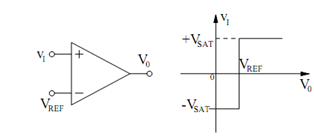
Non-inverting Comparator:
Figure (a) illustrates the circuit diagram of an op-amp utilized as a non-inverting comparator. The output voltage of the circuit is given by
v0 = VSAT sgn (VI - VREF )
The graph of v0 versus vI is given in Figure
(a) (b)
Figure: (a) Non-inverting Comparator; and (b) Plot of v0 Versus vI.
Positive feedback is frequently utilized with comparator circuits. The feedback is applied through the output to the non-inverting input of the op-amp. It is in contrast to the circuits covered in the preceding sections where feedback is applied to the inverting input. (The non-inverting integrator is an exception that uses feedback to both op-amp inputs.) Figure (a) gives the circuit diagram of an inverting op-amp comparator with positive feedback. The circuit is also called as a Schmidt trigger. The capacitor CF in the figure is supposed to be an open circuit in the following. This capacitor is frequently used to develop the switching speed of a comparator by enhancing the amount of positive feedback at high frequencies. It has no effect on the input voltage at which the op-amp switches states.
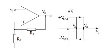
(a) (b)
Figure: (a) Inverting Comparator with Positive Feedback; and (b) Plot of v0 Versus vI.
The output voltage from the circuit of Figure (a) may be written
v0 = VSAT sgn (V+ - VI )
Because v0 has two stable states, v0 = +VSAT and v0 = - VSAT, it follows that vI may have two stable states given by
VA = V REF ( RF / (RF +R1) ) - VSAT (R1 /RF + R1)
VB = V REF ( RF / (RF +R1) ) - VSAT (R1 /RF + R1)
where superposition and voltage division have been used for each equation. For
vI < VA, it follows that v0 = +VSAT. For vI > VB, it follows that v0 = - VSAT. For VA < vI < VB, v0 may have two stable states, i.e. v0 = ± VSAT. The graph of v0 versus vI is given in Figure (b).
The value of v0 for VA < vI < VB based on whether vI enhance from a value less than VA or vI reduce from a value greater than VB. that is, the circuit has memory. If vI < VA, primarily and vI starts to increase, v0 remains at the + VSAT state until vI becomes greater than VB. At this point, v0 switches to the - VSAT state. If vI > VB primarily and vI starts to decrease, v0 remains at the - VSAT state until vI becomes less than VA. Then v0 switches to the + VSAT state. The path for v0 on the graph in Figure (b) is mentioned with arrows. The loop in the graph is commonly called a hysteresis loop.