Flip-Flops:
Flip-flops are utilized in building counters and registers and other sequential circuits.
Flip-flops are digital circuits whose output value shall not change once it is set unlike the combinatorial circuits whose output values is based on the input values. They are utilized for storing binary numbers and they are memory elements for sequential circuits. There are four fundamental Flip-Flops viz. SR-, JK-, T- and D-type Flip-Flops. We shall learn them one by one and explore their possible applications in digital circuits. Any device or circuit which has two stable states are called bistable such as switch has two states either it is up or down. Whereby it is up it is connected to Vcc (high) and when it is down it is connected to ground (low). Flip-flops also have two states of operation. When the flip-flop has output set to 0 V, it can be assumed as storing logic 0 and whereas the output is set to 5 V (Vcc), this is storing logic 1. Since a Flip-flop holds or latch into either one of these states this is also called as a latch. A basic Flip-flop or latch is achieved by cross-coupling two NOT circuits NOT-1 and NOT-2 as illustrated in Figure. Note down that single-input NAND gates perform the function of NOT gates. Do note that the Flip-Flop in Figure also has feedback line that means. output in each gate is connected to the input of the others. The output bistable states are depicted using Q = 1 ( Q¯ = 0) is called the 1 state and Q = 0 ( Q¯ = 1) is called the 0 state. It must be noted down that the outputs Q and Q¯ are always complementary for all cases.
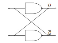
Figure: Basic Flip-Flop or Latch
An S¯ R¯ Flip Flop may be realized by using two NAND gates as shown in Figure (a) and its logic symbol is illustrated in Figure (b). Let us attempt to understand the truth table of S¯ R¯ Flip Flop drawn in Figure (c). We know that a low input on the NAND gate shall set the output high. Therefore a low on the input S¯ shall set the latch Q = 1 (Q¯ = 0) whereas a low on the R input will reset the latch Q = 0 ( Q¯ = 1). A high on both the inputs will make the outputs to the previous state. But a low on both the inputs will make the outputs Q = 1 (Q¯ = 1) which is forbidden. SR Flip Flop can be realized from the S¯ R¯ Flip Flop with the help of two single input NAND gates (inverters) at the input of S¯R¯ Flip Flops as illustrated in Figure (a). This S-R Flip Flop is an asynchronous circuit as it is independent of clock for its working. An S-R Flip Flop can be modified to a synchronous circuit by changing the connections as illustrated in Figure (b). If Clock = 0, both the input NAND gates NAND-3 and NAND-4 are disabled and the circuit is disabled. If Clock = 1, the circuit shall behave like a normal S-R Flip
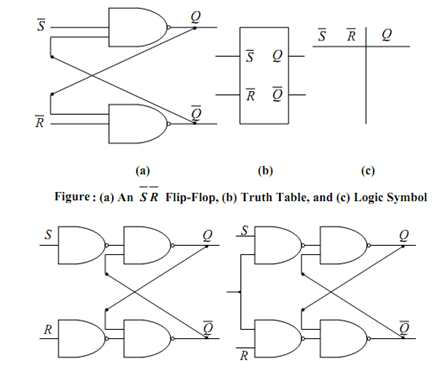
(a) (b)
Figure: (a) An S-R Flip-Flop from S R Flip Flop, and (b) Clocked S-R Flip Flop