Working of Junction:
When N-type material is negative with respect to P-type, as in the Figure A given below, electrons flow easily from N to P. The N-type semiconductor that already has an excess of electrons, gets even more; the P-type semiconductor, having a shortage of
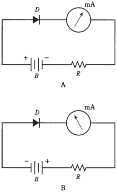
Figure--Series connection of battery B, resistor R, milliammeter mA, and diode D. At point A, forward bias results in current flow; at point B, reverse bias results in no current.
electrons, is made more deficient. The N-type material constantly feeds the electrons to P-type in an attempt to create electron balance, and battery or power supply keeps robbing electrons from P-type material. This is shown in the Figure A given below and is called as forward bias.
When polarity is switched so N type material is positive with respect to P type, things get interesting. This is known as reverse bias. Electrons in N-type material
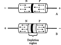
Figure- At point A, forward bias of a P-N junction; at point B, reverse bias. Electrons are shown as small dots, and holes are shown as open circles.
are pulled towards positive charge, away from junction. In P-type material, holes are pulled toward negative charge, also away from junction. The electrons (in N-type material) and holes (in P type) are the majority charge carriers. They become depleted in vicinity of P-N junction as shown in the figure B given below. A shortage of majority carriers means that the semiconductor material cannot conduct properly. Therefore, the depletion region behaves like an insulator.