Silicon-controlled Rectifier:
The silicon-controlled rectifier is 4-layer device with alternating p-type and n-type layers as illustrated in Figure (b). This device is also referred to as a Thyristor or pnpn structure and its symbol is drawn in Figure (a). Silicon thyristors are the most common thyristors. The plus point of the structure is that it gives high blocking voltage, a high power handling capability, and high gain with extremely low on-state resistance. The operation of the device is best described by considering the equivalent circuit, illustrated in Figure (d) and Figure (c) illustrates how a thyristor may be represented as two interconnected-transistors. It consists of two bipolar transistors, pnp transistor, T1, and a npn transistor, T2. Both transistors share n-type and p-type layer. For example, the p-type base layer of transistor T2 is also the collector layer of transistor T1, while the n-type base of transistor T1 is also the collector of transistor T2. The thyristor is controlled through the gate electrode which is the gate of T2. By applying a current to the gate one forward biases the base-emitter junction of T2, which leads to a collector current in T2 that in turn provides a base current to T1. As T1 is a complementary p-n-p transistor, this negative current also forward biases the base-emitter junction of transistor T1, resulting in collector current which compose an additional base current to the base of transistor T2. The applied current to the gate of the thyristor, thus, causes an additional current into T2, which can be large sufficient that both transistors remain turned on even if the original gate current is removed. This self- sustaining effect or latching behaviour shall occur if the product of the current gain of both transistors equals unity, while one of the transistors may have a current gain less than unity. Consequently one has considerable flexibility to select the doping density and thickness of each layer to obtain a high blocking voltage and high early voltage for each of the transistor, whereas maintaining enough current gain. The thyristor has low on-state voltage and an even smaller turn-on current, which only require to be applied temporarily due to the internal positive feedback among the two transistors of the equivalent circuit. This latter on property is also the main disadvantage of the thyristor : as the device latches into the on-state once sufficient gate current is supplied, the device may not be turned off by removing the gate current. Instead one ought to disconnect the power supply to turn off the device. In addition, since both of the transistors are in saturation in the on state, an important amount of minority carriers are accumulated in the base region of each transistor. These minority carriers should be eliminated prior to reconnecting the power supply as these carriers would temporarily lead to a base current in each of the device and trigger the turn-on of the thyristor. At last, one has to gradually ramp up the power supply voltage to ignore the so-called dV/dt effect. As a rapid enhance of the applied voltage with time causes a displacement current proportional to the capacitance of the junctions, it displacement current could again provide a temporary base current in T2 and T1, that is large sufficient to trigger the thyristor.
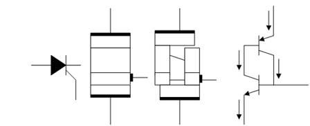
(a) (b) (c) (d)
Figure: (a) SCR Symbol; (b) SCR Structure; (c) SCR as a Two Inter-connected Transistors; and (d) Equivalent Circuit