MOS Transistor in Linear Range:
At the drain end of the channel, while Vds just equals Vdsat, the difference among the gate voltage and the channel voltage, Vgc (L) is just equal to VT, the threshold voltage. Any further enhance in Vds and the difference among the gate and the channel (in the channel region just near the drain) shall drop below the threshold voltage. It means that when Vds gets bigger than Vdsat, the channel just close the drain region disappears. We no longer have adequate voltage between the gate and the channel region to maintain an inversion layer, so simply we revert to a depletion condition. It is called pinch off. What happens to the drain current when we hit pinch off? It looks like it may go to zero, but that is not the right answer. Though there is no active channel in the pinch-off region, still there is silicon - it just happens to be depleted of all free carriers. There is electric field, going through the drain to the channel, and any electrons that move along the channel to the pinch-off region are dragged across by the field, and enter the drain. It is just like the current that flows in the reverse saturation condition of a diode. There are no free carriers in the depletion region of the diode, yet Isat does pass across the junction region. Under pinch-off conditions, further increases in Vds does not result in more drain current. You may think of the pinched-off channel as a resistor, along a voltage of Vdsat across it. When Vds gets higher than Vdsat, the excess voltage appears across the pinch-off region, and the voltage across the channel remains permanent at Vdsat. If the channel keeps the same charge, and contain the same voltage across it, then the current through the channel (and into the drain) shall remain fixed, at a value we shall call Idsat. Imagine we have a MOS field effect transistor which has a width of 10 microns, threshold voltage of 2 volts, and a channel length of 1 micron, oxide thickness of 150 angstroms, and a surface mobility of 400 cm2/V-s using εox = 3.3 × 10- 13 F/cm2, we get a value of 2.2 × 10⁻⁷ F/c for cox. Then this makes k have a value of
k = μs Cox W/L = ( 400 × 2.2 × 10-7 10) /1= 8.8 × 10- 4 A/V2
Let us consider the test circuit of Figure (a). In this case, Vds is kept fairly small (0.2 Volts or so) and the gate voltage Vgs is swept over some range. We have
I d = μs Cox WVds (Vgs - VT ) /L
This equation shall obviously give us a linear plot of Id as a function of Vgs, which shall look like as in Figure (b). Clearly, it is a device with a threshold voltage of about 2 volts.
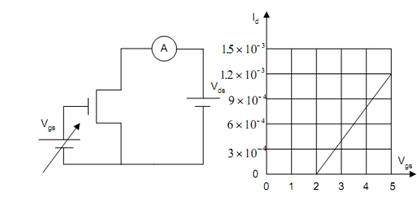
(a) (b)
Figure: (a) Circuit for Finding VT; and (b) Id as a Function of Vgs for a MOS Transistor in its Linear Range