In this activity, you are going to place components on a sheet and connect them with virtual wires to create a simple digital circuit. You will simulate the circuit to verify the correct behavior and measure the timing. Then you will program the Cyclone II FPGA on the DE1 board and demonstrate the correct circuit operation.
The function is ledr0 = sw0 OR sw1.
1. Create a new project.
First time setup: When you open Quartus II for the first time it will ask you what look and feel you would like. Choose the Quartus II option.
To begin a new project, select File -> New Project Wizard.... Select Next > at the first
|
screen.
|
ee310\lab1
|
|
|
What is the working directory for this project?:
|
|
|
What is the name of this project?
|
lab1
|
|
|
What is the name of the top-level design entity for this project?
|
or2in
|
|
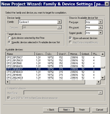
Click Next twice. This will bring you to the device selection screen. In the combo box to the right of Family:, choose Cyclone II. This will bring up the Cyclone II family part numbers. Select the EP2C20F484C7, then click Finish.
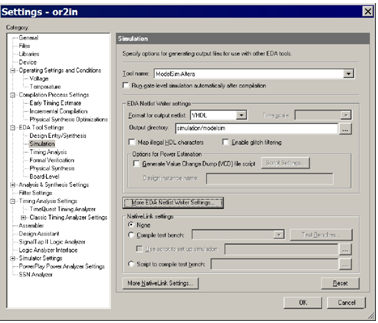
Specify that you will use the ModelSim simulator. Select Assignments > Settings... then select Simulation under EDA Tool Settings and select ModelSim-Altera for the Tool Name:. Click OK.
2. Enter the Design
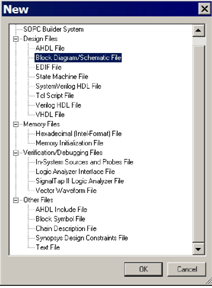
Select File > New > Block Diagram/Schematic File to create a new Block Diagram/Schematic File.
Add a new gate by clicking on the add symbol icon (the AND gate) in the toolbar to the left of the working area. You can also double click in the drawing area. In the list box below Libraries:, click on the expand (+ ) icon to the left of c:/altera/quartus/libraries/ to display the available libraries. Expand the primitives library, then the logic library.
Select the or2 symbol in the list of the logic library. You should now see the symbol for an OR gate with 2 inputs. Click OK . You are now ready to place an or2 gate. Click somewhere in the working area to create an instance of the or2 gate in your schematic.
3. Name the Input and Output Pins
Again, select the add symbol icon. This time open the primitives/pin library . Select the output symbol and click OK. Put the output pin to the right of the or2 gate. Cancel the insertion of the output pin. Repeat with two input pins.
To connect the pin symbols to the or2 symbol, place the mouse at the end of one of the wires in the symbols, your cursor should turn into a + sign and there should be a + below and to the right of your cursor. Once you have the correct cursor click and drag to the wire you wish to connect to. A box will appear around the end of the wire you are connecting to, place your cursor inside this box and release the mouse button. Using this method, connect each of the input and output pins to the logic symbol.
To name a pin, right click on the pin and select Properties. There will be a text box labeled Pin name(s):, this is where you enter the name of the pin. After you have entered the name of the pin, click OK.
You will be creating a circuit to turn on ledr0, the first red led, when switch 0, switch 1, or both are in the on position. Therefore, name the two input pins sw0 and sw1 and the output pin ledr0. You are now done creating the schematic. Save as or2in.bdf. The next step is to assign pins in the schematic to physical pins on the FPGA.
4. Compile the Design
Now save your design, and then compile it using Processing > Start Compilation. The compilation will take a long time. You can watch the progress in the Status window on the left. A dialog will pop up when it is done. Ignore any warnings for now.
5. Enter the Hardware Pin Assignments
Select Assignments > Pins from the menu. This brings up the pin assignment dialog box. We will be assigning sw0 and sw1 to pins PIN_L22 and PIN_L21, respectively, and ledr0 to pin PIN_R20. To do this, find the list of the symbolic pin names you defined earlier (they will be in the Node Name column), and double click in each pin's Location column. This will show a drop down list of the physical pins available, e.g., PIN_L22. Selecting a pin will assign it to the net it is to the right of. You can also type in the pin name. Now close the Pin Planner panel.
Important: After setting up each of the nodes to its proper physical pin, all other pins should be set to inputs so that they will not conflict with any of the other devices on the board. To do this, select Assignments > Device..., then click on Device and Pin Options.... Select the Unused Pins tab. In the combo box labeled Reserve all unused pins:, select As input, tri-stated. Click OK twice.
Now save and compile again. There should be no errors and only one warning, saying, Warning: Found 1 output pins without output pin load capacitance assignment (You can click on the Warnings tab to check after compilation is completed). This indicates a successful compile. The next step is to simulate the design to prove correctness.