Reference no: EM131074091
Introduction:
Write one to two paragraphs about the Lab. Explain the following information for this lab:
- What are the goals to achieve in the lab?
- What are the expectations of the lab?
- How will you be implementing this lab?
- What will you try to measure?
Equipment/Components:
Listthe type of equipment or components that you will be using? Where will you find these components? How will you use these components in Multisim/VHDL? Explain any adjustments required such as tolerances.
Procedure:
Briefly describe how you will approach the problem and try to solve the lab, describe and explain any techniques/rules/laws/principles you would use. Outline each step of the process.
Circuit design:
Take a screenshot of the circuit/logic from Multisim/VHDL as asked in the lab assignment before you run the circuit and paste it here in your report.
Execution/Results:
Run the circuit in Multisim/VHDL and copy/paste the results from the simulationincluding any readings, plots or graphs.
Copy/Paste the screenshots for all the measurements required in the lab here. Be sure to add a title and explain what each of the screenshots represent.
Analysis:
Analyze the results obtained from Multisim/VHDL and compare those to your calculated results (if required).
Answer the following questions:
- What did you discover/confirm?
- Use tables and diagrams to record results.
- Compare calculations with the measured values.
- Analyze your results.
Explain if your simulation is correct or incorrect and why. If the results are confirmed, then your measurements are correct. If they are not confirmed, explain what the problem is. You will need to discuss how to troubleshoot the circuit to achieve the correct results.
Conclusion:
Summarize the entire lab in 1 to 2 paragraphs with the results and analysis in mind.
Answer any questions asked in the lab assignment here.
Cite any sources that you may use in your report.
Please download this document and type in your answers for questions in parts 1 and 2; save this document using the following format: CE212Lab6firstname_lastname.doc.
Introduction
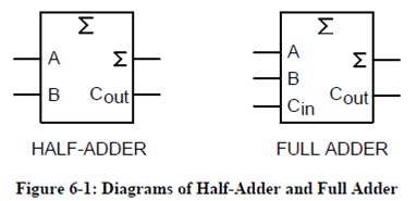
One class of combinational logic consists of decision circuits, in which the circuit evaluates the input signals todetermine which specific action to take. The 2-of-3 voting logic circuit in Experiment 5 is an example of adecision circuit. Another important class of combinational logic consists of arithmetic functions, in which thecircuit processes numeric (binary) data. Many of the earliest digital circuits were designed to perform highspeedcalculations, and arithmetic functions today are found in a wide variety of calculating and measuringdevices. The basis of arithmetic functions is a device called the adder, which, as its name suggests, adds twobits. There are two basic varieties of adders, called the half-adder and full adder.
The half-adder has two inputs, corresponding to two input bits, and two outputs, which indicate the sum andcarry that result from adding the two input bits. A limitation of the half-adder is that it cannot add groups ofbits, as the carry from one column cannot propagate to the next column. The full adder is similar to the halfadderbut adds a third input, called the carry in. The carry in allows the full adder to accept the carry bit from a previous adder so that groups of bits can be added. Figure 6-1 shows the diagram of a half-adder and full adder.
In Part 1 of this experiment, you will examine and verify the operation of a full adder circuit. In Part 2, you will examine how a 4-bit full adder is cascaded to add 8-bit and wider numbers.
Reading
Kleitz, Digital Electronics: A Practical Approach with VHDL, 9th Edition, Chapter 5.
Multisim Files
Part 1: Digital_Exp_06_Part_01a and Digital_Exp_06_Part_01b
Part 2: Digital_Exp_06_Part_02a, Digital_Exp_06_Part_02b, and Digital_Exp_06_Part_02c
Key Objectives
Part 1: Examine, verify, and compare the gate-level implementations of the full adder.
Part 2: Examine and verify the operation of cascaded 4-bit binary adders.
Part 1: The Full-Adder
6.0 Implementation 1
1) For each row in Table 6-1, record the expected sum and carry values for the "Cin", "A" and "B" inputs for a full adder in the "Σ" and "Cout" columns.
2) Open the Multisim file Digital_Exp_06_Part_01a.
3) Start the simulation.
4) Use the "A", "B", and "C" keys to open and close the "Input A", "Input B", and "Carry In" switches for
each of the settings shown in Table 6-2. Alternatively, you can click on the switches to open or close them.
5) Record the state of the "Sum" and "Carry Out" probes for each combination of switch settings in the "Σ" and "Cout" columns of Table 6-2.
6) Stop the simulation.
Table 6-1: Sum and Carry Outputs for Full Adder
|
Cin
|
A
|
B
|
∑
|
Cout
|
Cin
|
A
|
B
|
∑
|
Cout
|
|
0
|
0
|
0
|
|
|
1
|
0
|
0
|
|
|
|
0
|
0
|
1
|
|
|
1
|
0
|
1
|
|
|
|
0
|
1
|
0
|
|
|
1
|
1
|
0
|
|
|
|
0
|
1
|
1
|
|
|
1
|
1
|
1
|
|
|
Table 6-2: Observed Outputs for Full Adder Implementation 1
|
Cin
|
A
|
B
|
∑
|
Cout
|
Cin
|
A
|
B
|
∑
|
Cout
|
|
0
|
0
|
0
|
|
|
|
1
|
0
|
0
|
|
|
0
|
0
|
1
|
|
|
|
1
|
0
|
1
|
|
|
0
|
1
|
0
|
|
|
|
1
|
1
|
0
|
|
|
0
|
1
|
1
|
|
|
|
1
|
1
|
1
|
|
6.2 Implementation 2
1) Open the Multisim file Digital_Exp_06_Part_01b.
2) Start the simulation.
3) Use the "A", "B", and "C" keys to open and close the "Input A", "Input B", and "Carry In" switches for
each of the settings shown in Table 6-3. Alternatively, you can click on the switches to open or close them.
4) Record the state of the "Sum" and "Carry Out" probes for each combination of switch settings in the "Σ"and "Cout" columns of Table 6-3.
5) Stop the simulation.
|
Cin
|
A
|
B
|
∑
|
Cout
|
Cin
|
A
|
B
|
∑
|
Cout
|
|
0
|
0
|
0
|
|
|
|
1
|
0
|
0
|
|
|
0
|
0
|
1
|
|
|
|
1
|
0
|
1
|
|
|
0
|
1
|
0
|
|
|
|
1
|
1
|
0
|
|
|
0
|
1
|
1
|
|
|
|
1
|
1
|
1
|
|
Questions for Part 1
1) How could you configure a full adder to operate as a half-adder?
2) Do the outputs of the full adders in Table 6-2 and Table 6-3 match the expected values in Table 6-1?
3) What advantage, if any, does the full adder in Digital_Exp_06_Part_01b have over the full adder in
Digital_Exp_06_Part_01a?
Part 2: Parallel Binary Adders
The 7483 is a 4-bit parallel binary adder that can add two sets of 4-bit binary numbers. This device has carry in(C0) and carry out (C4) pins that allow you to cascade two or more devices to form 8-bit and wider adders.
6.3 Cascaded 8-Bit Adder
1) Calculate the sum for the "Input A" and "Input B" values for each row in Table 6-4 and record your
answer as a three-digit hexadecimal value in the "Calculated Total" column. The first value is already
given.
2) Open the Multisim file Digital_Exp_06_Part_02a.
3) Start the simulation.
4) Use the "Input A" and "Input B" DIP switches to apply each of the hexadecimal inputs in Table 6-4 to
the adder circuit.
5) For each setting in Table 6-4, record the "Overflow" state as "ON" or "OFF" and the hexadecimal
"Sum" value. What is the largest value the circuit can display without an overflow indication?
FF hexadecimal (255 decimal).
6) Stop the simulation.
Table 6-4: Results for 8-bit Adder (Values are in hexadecimal)
|
Input
A
|
Input
B
|
Calculated
Total
|
Overflow
|
Sum
|
Input
A
|
Input
B
|
Calculated
Total
|
Overflow
|
Sum
|
|
00
|
00
|
000
|
|
|
80
|
80
|
|
|
|
|
1F
|
2B
|
|
|
|
AA
|
BB
|
|
|
|
|
39
|
64
|
|
|
|
CA
|
FE
|
|
|
|
|
7F
|
80
|
|
|
|
FF
|
FF
|
|
|
|
Compare your "Calculated Total" value with the "Overflow" and "Sum" values for each row in Table
6-4. What does the binary value of "Overflow" indicator represent?
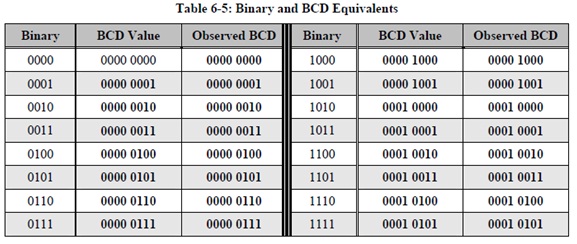
6.6 4-Bit Binary-to-BCD Converter
1) For each binary value in Table 6-5, indicate the corresponding 2-digit BCD value in the "BCD Value"
column. The first value is already given.
2) Open the Multisim file Digital_Exp_06_Part_02b. Note that three of the BCD value probes connect to
ground and never light up. Why are these probes included in the circuit if they are always OFF?
3) Start the simulation.
4) Use the DIP switch to apply each of the binary values in Table 6-5 to the converter circuit and record the resulting BCD pattern in the "Observed BCD" column.
5) Stop the simulation.
6.9 6.9 8-bit Binary-to-Decimal Converter
The 4-bit binary-to-BCD converter can be expanded to an 8-bit binary-to-decimal converter, although the design approach is more complex. In effect, the circuit independently adds the ones, tens, and hundreds represented by each bit in binary. It uses the basic circuitry for the 4-bit binary-to-BCD converter to adjust each sum as needed to keep the result in BCD, and adds the appropriate carries for each BCD digit to the next higher digit. Each BCD value is then displayed as a decimal digit.
1) Open the Multisim circuit Digital_Exp_06_Part_02c.
2) Start the simulation.
3) Use the DIP switch to apply each of the binary values in Table 6-6 to the converter circuit and record the resulting decimal value in the "Observed Value" column.
4) Stop the simulation.
Table 6-6: Corresponding Binary and Decimal Values
|
Binary Value
|
Decimal Value
|
Observed Value
|
Binary Value
|
Decimal Value
|
Observed
Value
|
|
00000001
|
|
|
10101010
|
|
|
|
00010000
|
|
|
11000011
|
|
|
|
01100100
|
|
|
11111111
|
|
|
How do the conversion times for the combinational binary-to-decimal converter compare with the conversion time for the sequential binary-to-decimal converter in Experiment 2?
Questions for Part 2
1) The AND gates in Digital_Exp_06_Part_02a serve to buffer the DIP switch settings for the hexadecimal displays. One input of each 2-input AND gate between the input DIP switches and rest of the circuit is tied to VCC (logic 1). Does this change the logic state of the DIP switch settings seen by the adders?
2) How would you modify the circuit in Digital_Exp_06_Part_02a to create a 12-bit adder? What additional parts would the circuit require?
3) How does the converter circuit of Digital_Exp_06_Part_02b convert the 4-bit binary value from the DIP switch to a BCD value?
4) Why do the digits on the displays in Digital_Exp_06_Part_02c sometimes briefly "flicker" when you change the DIP switch settings from one binary number to another?