Calculate the dimension of the channel width

Assignment Help Electrical Engineering
Reference no: EM131469642

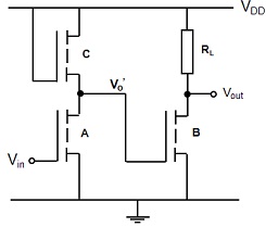
The design work involves producing layouts for circuit in Fig. 1. Such layouts correspond to the patterns developed on the masks, for use in the fabrication process, as discussed in lectures. Each of the layouts MUST be drawn on a graph paper with stipulated scale (e.g. 1µm per cm). The four masks that need to be defined are: device area, gate stripe, contacts and metal pattern. Produce individual layouts for each device i.e. A, B, C and RL, and also the overall layout for the circuit, in terms of the minimum feature size. Make sure to include the alignment errors between the layouts and minimise the area used.

Description: The circuit in Fig. 1 consists of a two-stage inverter, where the output from the 1st inverter Vo' is fed into the input gate of the 2nd inverter. The driver of both inverters consists of enhancement type n- MOS transistors A and B. Note these transistors have identical aspect ratios. It can be assumed that the threshold voltage VT to be 0.3 V. For the loads, the 1st inverter has an (active) saturated n-MOS transistor C, whilst the 2nd inverter has an (passive) implanted resistor load RL.
1415_Figure.jpg

Note the resistance value of C is equal to the resistance RL, and similarly, the resistance of A is identical to the resistance of B, when the transistors are on.

For your design, calculate the dimension of the channel width W for the drivers and respective dimensions of W and L for C and RL. To assist you with the calculation, you can select appropriate value for the output voltage Vo', which corresponds to the logic 0 condition, assuming a logic 1 input to be equal to VDD = 5 V. Note the value of Vo' needs to be lower than VT of the driver B in order to ensure that the transistor remains off at logic 0. The value depends on the ratio of the resistances between the driver and load for each inverter. Also for the implanted resistor RL, you can assume a sheet resistance of 150Ω/square, where each square is defined by minimum feature size. Note for the layouts you must take account the alignment accuracy λa, which can also be assumed to be equal to the minimum feature size. For your calculation, you can assume the following values for the parameters:

i. Minimum feature size λm = 0.5 µm
ii. Supply voltage VDD = 5V (Logic 1 input)
iii. Threshold voltage VT = 0.3 V
iv. Sheet resistance 150 Ω/square
v. Device constant is given as,

β = (μCo)W/L = (βo)W/L

where βo = 1.8 x 10⁻⁴ AV-2

For the Report: Give a brief description of the circuit operation in Figure 1. Include all your calculations and reasons for the assumptions made. Represent all respective individual and overall design layouts in scaled graph paper, in terms of minimum feature size. Use different shading to indicate the different regions and include the alignment errors between respective layouts.

Verified Expert

In the given question, a design was to be analysed mathematically and the values of resistances to be determined which has been done. Also, a layout was to be drawn on graph paper whose image I have attached.

Reference no: EM131469642

Questions Cloud

Discuss how an ethical egoist and utilitarian would respond : Discuss how an ethical egoist and a utilitarian would respond? Compare your responses to that of ethical egoism and and utilitarianism.
Find the optimal assignment of departments to locations : University of the Atlantic is moving its business school into a new building, which has been designed to house six academic departments.
Discuss viewpoints or opposing viewpoints to the program : Describe whether the program is effective and offer evidence to support your rationale. Discuss other viewpoints or opposing viewpoints to the program.
Write out the complete quadratic assignment formulation : Consider the following problem with two locations and three machines. Suppose that the costs of transporting a unit load from location j to location r.
Calculate the dimension of the channel width : Calculate the dimension of the channel width W for the drivers and respective dimensions of W and L for C and RL.
How does the given judgment differ from your own : Describe the deontological position on telling a lie to save the life of an innocent. How does this judgment differ from your own?
Briefly explain the craft cofad and corelap : Briefly describe each of the following computerized layout techniques. In each case, indicate whether the method is a construction or improvement method.
Find the centroids of a and d in the new layout : Consider the initial layout for Example, which appears in Figure 11-11. Draw a figure showing the layout obtained from exchanging the locations of A and D.
How would virtue theorist respond to this moral dilemma : How would virtue theorist respond to this moral dilemma? How would you respond and why? What did you learn from this thought experiment?

Reviews

len1469642

4/21/2017 6:47:39 AM

Following are the details and attachment provided by the student. Please be sure if your tutor can do the assignment or not. you should initially focus on the 1st inverter stage, and subsequently calculate the value for the ratio of (W/L)A to (W/L)C. You should then ‘select’ appropriate values for respective aspect ratio of the two devices, however making sure the calculated ratio of the two is maintained. When selecting the values, you need to take into account that appropriate alignment error is included within respective layouts, and also minimal area is utilised. You will thus find that the selection process for the respective aspect ratios can be reiterated. Make sure to include all your findings in the report. For the 2nd stage inverter, the driver A is the same as B, so the same aspect ratio applies. The load devices, C and RL have the same resistance however have different dimensions since one is a passive load and the other an active load. So you should work out appropriate value for L and W of RL.

Write a Review

Electrical Engineering Questions & Answers

  Define nmos fet and bjt analysis

A standard silicon NPN BJT is to be used as an amplifier. The emitter voltage is biased at 4 volts, the base is biased at 5 volts, and the collector is biased at 10 volts. Will this circuit perform as desired? Why or why not.

  Create a new mbed c-code project called intcount1

Use the Timeout class to provide a two second delay. During the delay, display the number of interrupts that are occurring on Pin 5 using LED1-LED4. LED1 is the low-order bit. Use only the BusOut class for driving the LEDs.

  Is this device p channel or n channel

Plot the transfer characteristic curve using the data from part (b).

  A total of 24 mhz of bandwidth is allocated to a

a total of 24 mhz of bandwidth is allocated to a particular fdd cellular telephone system that uses two 30 khz

  State the main requirements of a protection ct

State the main requirements of a protection CT and an instrument CT -  If the setting is 20% and there is saturation of 50% at 20 x current setting, specify a suitable CT.

  What is the amount of charge stored in the capacitor

A 1000-μF capacitor is fully charged to 10 V. What is the amount of charge stored in the capacitor. How much energy isstored.

  There are 15 randomly selected multiple choice questions

There are 15 randomly selected Multiple Choice questions

  Find the internal induced voltage and torque angle

Find the input torque to the generator.If armature current and field current are kept constant, find the new value of the terminal voltage if the power factor is changed to 0.7 lagging.

  Determine the increase in entropy per lbm

Determine the increase in entropy per lbm of R-134a flowing through the expansion valve and the entropy production rate per unit mass flow rate of R-134a flowing through the expansion valve.

  How are nozzles rated and what does oil viscosity mean

List the grades of fuel oil, and give a brief description of each type.

  Draw equivalent circuit of medium-length transmission line

How do the short length and medium length transmission line models differ and why Draw the equivalent circuit of a medium-length transmission line

  Write the nodal equations for the networks of given figure

Write the nodal equations for the networks of given figure. - Using determinants solve for the nodal voltages. - Determine the magnitude and polarity of the voltage across each resistor.

Free Assignment Quote

Assured A++ Grade

Get guaranteed satisfaction & time on delivery in every assignment order you paid with us! We ensure premium quality solution document along with free turntin report!

All rights reserved! Copyrights ©2019-2020 ExpertsMind IT Educational Pvt Ltd