JFET:
The JFET structure looks as Figure (a). It contains a piece of p-type silicon, into which two n-type regions have been diffused. Though, instead of being both on the same surface, as with a MOSFET, the two of regions are opposite to one another on either side of the crystal. In cross-section, the JFET looks as Figure (b). We also illustrate the biasing here.
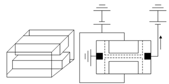
(a) (b)
Figure: (a) JFET; and (b) Biasing of JFET
The two n-regions are connected together, and are reverse biased w.r.t. the p-type substrate. A second battery, Vds, is utilized to pull current out of the source, by applying a negative voltage among the drain and the source. The reverse biased n-p junctions create a depletion region, which extends to the p-type material through which the holes travel as they go through source to drain (a channel). By adjusting the value of Vgs, one may make the depletion region smaller or larger, therefore increasing or decreasing the drain current. Note that the polarity of the Vds battery makes it so that there is more reverse bias across the p-n junctions at the drain end of the channel than at the source end. Therefore, a more accurate depiction of the JFET would be what is illustrated in Figure (a). While the drain/source voltage gets large adequate, the two depletion regions shall join collectively, and, just as with the MOSFET, the channel pinches off, as illustrated in Figure (b).
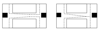
(a) (b)
Figure: (a) Depletion Region Controls Current; and (b) Pinch-off
By using JFETs is a little more cumbersome than a normal MOSFET. You should make sure that the gate-substrate junction always remains reverse biased, and as the JFET may only be a depletion-mode device, you need to have a voltage on the gate if you desire to turn the transistor off. The JFET does have one benefit over the MOSFET though. A while back we compute the value for Cox the oxide capacitance and found that it was on the order of 10- 7 Fcm2. A typical MOSFET gate may be 1 μm long by 20 μm wide, and so this would have a gate area of 20 μm2 or 2 × 10- 7 cm2. Therefore, the total gate capacitance is only about 10-14 F.