Random Access Memory (RAM):
RAM is the main memory of the computer. It controls the computer speed. Information may be randomly written or read from such memories and therefore the name Random Access Memory or RAM. We may use SR Type or JK Type Flip Flops to realize a RAM. Let us try to understand a basic element of RAM as depicted in Figure. To write down an input to the Flip Flop, we enable the inputs AND-1 and AND-2 by keeping it high. If the write input is 1 (0), then the S/J input is 1(0), R/K input is 0(1), Q value is 1 (0). To read an input, we make the Address line high, thus AND-3 is enabled and we read the output 1 (0) for this particular case.
A very simple kind of electronic memory is the bistable multivibrator. Capable of storing up a single bit of data, it is volatile (needing power to maintain its memory) and extremely fast. The D-latch is probably the simplest implementation of a bistable multivibrator for memory usage, the D input serving like the data "write" input, the Q output serving like the "read" output, and the enable input serving like the read/write control line as illustrated in Figure (a). If we want more than one bit's worth of storage (and we probably do), we ought to have many latches arranged in some kind of an array where we may selectively address which one (or which set) we're reading from or writing to. By using a pair of tristate buffers, we may connect both the data write input and the data read output to a common data bus line, and allow those buffers to either connect the Q output to the data line (READ), attach the D input to the data line (WRITE), or keep both buffers in the High-Z state to disconnect D and Q from the data line (unaddressed mode). One memory "cell" would seem like this, internally as illustrated in Figure (b). In Figure (c), while the address enable input is 0, both tristate buffers shall be placed in high-Z mode, and the latch shall be disconnected from the data input/output (bus) line. Only while the address enable input is active (1) shall the latch be connected to the data bus. Of course, every latch circuit will be enabled with a different "address enable" (AE) input line, which shall come from a 1-of-n output decoder. In the above circuit, 16 memory cells are individually addressed with a 4-bit binary code input into the decoder. If a cell is not addressed, it shall be disconnected from the 1-bit data bus by its internal tristate buffers: consequently, data may not be either written or read through the bus to or from that cell.
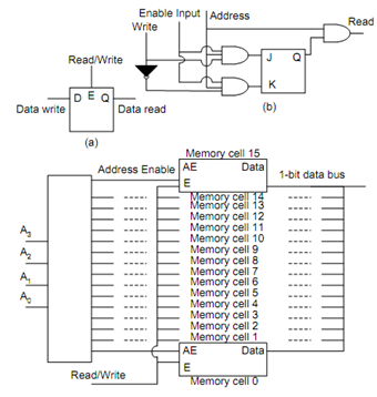
Figure: (a) A Simple RAM, (b) Basic RAM Cell, and (c) 16 × 1 Bit Memory