Reference no: EM132240229
Analog IC Design Assignment - MOSFET Review & Single Stage Amplifiers
Simulate the following using Cadence Virtuoso and the provided 130 nm technology files. Use thin-oxide devices (1.2V).
1. Plot ID - VGS characteristics for NMOS and PMOS devices.
a. Use W = 1μm, L = Lmin, VGS = 0: 10m: 1.2, and VDS = 1.2V.
b. Repeat for W = 10μm and L = 10Lmin.
c. Comment on the differences between (a) and (b).
2. Plot ID - VDS characteristics for NMOS and PMOS devices.
a. Use W = 1μm, L = Lmin, VDS = 0: 10m: 1.2, and VGS = 0: 0.2: 1.2.
b. Repeat for W = 10μm and L = 10Lmin.
c. Comment on the differences between (a) and (b).
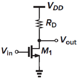
3. Simulate the CS amplifier shown below.
a. Use VDD = 1.2V and W/L = 10μm/10Lmin. Select RD such that Vout = VDD/2 at Vin = VDD/2. Report the following:
i. Vout vs Vin. Use DC sweep Vin = 0: 0.01: 1.2.
ii. Av vs Vin. (Hint: differentiate the previous plot using Cadence Calculator). What is the max gain? What is the valid input and output voltage range such that the gain is within 20% of the max value?
iii. ID vs Vin.
b. Repeat while adding a source resistance RS = RD/4. Note that you need to reselect appropriate RD.
c. Comment on the differences between (a) and (b).