Reference no: EM132190965
Question 1)
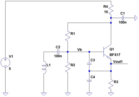
a) What amplifier topology does Q1 form, i.e. common-base, etc.
b) Select component values for the above oscillator to produce a 100 MHz sinewave with low distortion and 1 Vp-p amplitude at Vout1. Use any combination of analysis and simulation, However, your design choices must be well justified.
Note: R3 sets the bias current for Q1, and is also known as a gain compression resistor since it can be used to tune the magnitude of oscillation.
c) Validate your design by simulation
d) Plot the spectrum and measure the harmonic distortion, caused by the first three harmonics.
e) Simulate the effect of connecting a dipole antenna to Vout1 that is operating at resonance with a 250-Ohm radiation resistance. Is the additional load acceptable?
f) To reduce the loading effect on Q1, design an emitter follower stage, designed to drive a 250- Ohm antenna with 1 Vp-p.
g) Simulate the response and remeasure the harmonic distortion at the antenna? How will the impedance of the antenna effect the harmonics? That is, is an output filter required?
h) What is the transmitted power?
Question 2)
a) Design a 50-Ohm LC filter with a 20-MHz passband and centre frequency of 100 MHz. The attenuation should exceed 20 dB at frequencies more than 40 MHz away from the centre frequency. Use real components available from Element14.
b) Plot the magnitude and phase response of the forward voltage gain (S21). Does the response satisfy the specification?
Question 3)

The shaded area of the above circuit represents a resistive half-bridge strain sensor. When the sensor is exposed to a strain ∈, the resistances become R1 = R(1 + ∈) and R2 = R(1 - ∈), where
R is the nominal resistance.
• The opamp has a gain-bandwidth product of 10 MHz, and a first-order response.
• The opamp noise sources are vn = 10 nV/√Hz, in+ = i- = 1 ρA/√Hz
• The strain is ∈ = ±0.001, and R = 100Ω
a) Derive the relationship between ∈ and Vout.
b) What is the noise density (in nV/√Hz) at Vin due only to R1 and R2?
c) What is the noise density (in nV/√Hz) at Vout due to the opamp noise sources?
d) What is the noise density (in nV/√Hz) at Vout due to R3 and R4?
e) List the noise contributions at Vout (in nV/√Hz), and identify the most significant source.
f) Choose values for R3 and R4 so that the output is ±10 V when ∈ = ±0.001.
g) Calculate the RMS noise at the output, due to the amplifier and source resistances.
h) Calculate the noise factor and noise figure. Describe the significance.
i) Calculate the resolution at the output, as a percentage of the peak-to-peak noise and signal.
j) To sample the output with a microcontroller ADC, would you use a 10, 12, 14, or 16 bit ADC?
k) Calculate the signal-to-noise ratio at the input and output when ∈ = 0.001 sin(2Π100t).
l) Find the spectral density of Vout and RMS noise by simulation. Compare to the value from G).
m) Plot the individual contributions to the output noise spectral density (by simulation).
n) Select a suitable opamp that will result in a bandwidth of 3 kHz or greater.
o) Estimate the peak-to-peak 1/f noise at the output in the bandwidth of 0.1 - 10 Hz or similar. (Hint: use the low-frequency noise specifications in the opamp datasheet)
Question 4)
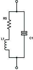
A coil antenna for a 100 MHz transmitter looks like the above impedance.
• L1 = 0.1 uH, R5 = 10 Ω, C1 = 10 pF
a) Calculate the impedance at 100 MHz.
b) Plot the normalized impedance at 100 MHz on a Smith Chart, based on Z0 = 50 Ω
c) Show that the impedance can be matched by a parallel resistance and series capacitor by plotting the course to z = 1 on the Smith chart
d) Find the exact required matching component values at 100 MHz
e) Using a circuit simulator or QuickSmith, plot the normalized impedance of the network before and after matching, from 1 MHz to 1 GHz.
f) In words, qualitatively describe the characteristics of the matched impedance as a function of frequency. That is, what does it look like at low and high frequencies etc.
Question 5)
A 50 Ω transmission line is driven by a source impedance of 50 Ω and terminated imperfectly by a 50 Ω resistor in parallel with a 5 pF capacitor.
• Transmission line length = 10 cm, Velocity = 0.5c
a) Using a simulation tool, plot the normalized impedance of the load from 10 MHz to 2 GHz.
b) Using a simulation tool, plot the normalized input impedance of the transmission line from 10 MHz to 2 GHz. Describe the response.
c) What effect does changing the transmission line length have, for example at 1 GHz? Can this be used to match the impedance?
d) Plot the frequency response form the source voltage to the load voltage using a simulator from 10 MHz to 2 GHz.
e) Replot the frequency response when the load capacitance is 1 pF and 0.1 pF. Comment on the importance of precise termination at high frequencies.