Find the small-signal output resistance

Assignment Help Electrical Engineering
Reference no: EM132185363

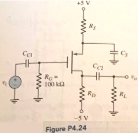
Question 1 - For the common-source circuit in Figure P4.24, the bias voltages are changed to V+ = 3 V and V- = -3 V. The PMOS transistor parameters are: VTP = -0.5 V, Kp, = 0.8 mA/V2, and λ = 0. The load resistor is RL =  2 Ω ka (a) Design the circuit such that IDQ = 0.25 mA and VSDQ = 1.5 V. (b) Determine the small-signal voltage gain Av = vo/vi.

12_figure2.jpg

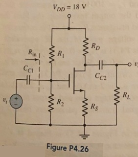
Question 2 - Design the common-source circuit in Figure P4.26 using an n-channel MOSFET with λ= 0. The quiescent values are to be IDQ = 6 mA, VGSQ = 2.8 V, and VDSQ = 10 V. The transconductance is gm = 2.2 mA/V. Let RL = 1 kΩ Av = -1, and Rin = 100 KΩ. Find R1, R2, RS, RD, Kn, and VTN.

102_figure3.jpg

Question 3 - Consider the circuit in Figure P4.34. the transistor parameters are VTN = 0.6 V, kn' = 100μ A/V2, and λ = 0. The circuit is to be designed such that VDSQ = 1.25 V and such that the small-signal voltage gain is Av = 0.85. (a) Find IDQ. (b) Determine the width-to-length ratio of the transistor. (c) What is the required dc value of the input voltage?

148_figure.jpg

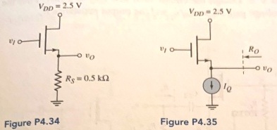
Question 4 - The quiescent power dissipation in the circuit in Figure P4.35 is to be limited to 2.5 mW. The parameters of the transistor are VTN = 0.6 V, kn' = 100 μA/V2, and λ = 0.02 V-1. (a) Determine IQ. (b) Determine W/L such that the output resistance is Ro = 0.5 kΩ. (c) Using the results of parts (a) and (b), determine the small-signal voltage gain. (d) Determine the output resistance if the transistor width-to-length ratio is W/L = 100.

Question 5 - The parameters of the circuit in Figure P4.36 are Rs = 4 kΩ, R1= 850 kΩ, R2 = 350 kΩ, and RL = 4 kΩ. The transistor parameters are VTP = -1.2 V, kp' = μA/V2 W/L = 80, and λ = 0.05 V-1. (a) Determine IDQ and VSDQ (b) Find the small-signal voltage gain Av = vo/vi. (c) Determine the small-signal circuit transconductance gain Ag = io/vi. (d) Find the small-signal output resistance Ro.

1404_figure1.jpg

Question 6 - The small signal parameters of the NMOS transistor in the ac equivalent common-gate circuit shown in Figure p4.47 are VTN = 0.4 V, k'n = 100 μA/V2 W/L = 80 and λ = 0 The quiescent drain current is IDQ = 0.5 mA. Determine the small-signal voltage gain and the input resistance.

903_figure4.jpg

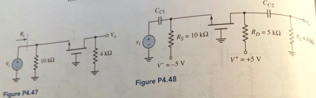
Question 7 - For the common-gate circuit in Figure P4.48, the NMOS transistor pares am: VTN =1 V, Kn = 3 mA/V2, and λ = 0. (a) Determine IDQ and VDSQ (b) Calculate gm and r0. (c) Find the small-signal voltage gain Av = vo/vi.

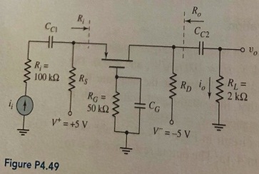
Question 8 - Consider the PMOS common-gate circuit in Figure P4.49. The transistor parameters are: VTP = -1 V, Kp = 0.5 mA/V2, and λ = 0. (a) Detemine RS and RD such that IDQ = 0.75 mA and VSDQ = 6 V. (b) Determine the input impedance Ri, and the output impedance Ro. (c) Determine the loaf current 4, and the output voltage vo, if = 5 sin ωt  μA.

2326_figure5.jpg

Question 9-  The transistor parameters in the circuit in Figure P4.68 are the same as those given in Problem 4.68. The circuit parameters are VDD = 3.3 V, Rs1 = 1kΩ, and Rin = 250 kΩ. (a) Design the circuit such that tDQ1 = 0.1 mA, /n(: = 0.25 mA, Vpsei = 1.2 V. and ViDQ2 = 1.8 V. 0)) Determine the small-signal voltage gain Av = vo/vi

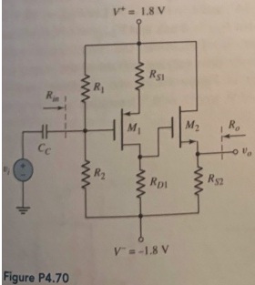
Question 10 - Consider the circuit shown in Figure P4.70. The transistor parameters are VTP1 = -0.4 V, VTN2 = 0.4 V. (W/L)1= 20, (W/L)2 = 80, k'p= 40 μA/V2 k'n = 100 μA/V2 and λ1 = λ2 = 0. Let = 200kΩ. (a) Design the circuit such that IDQ1= 0.1 mA, IDQ2 = 0.3 mA. VSDQ1 = 1.0 V and VDSQ2 = 2.0 V. The voltage across RS1 is to be 0.6 V. (b) Determine the small-signal voltage gain Av = vo/vi,. (c) Find the small-signal output resistance Ro.

491_figure6.jpg

Question 11 - For the circuit in Figure P4.71, the transistor parameters are: Kn1 = kn2 = 4 mA/V2, VTN1 = VTN2= 2 V. and I = A2 O. (a) Determine IDQ1, IDQ2, VDSQ1, and VDSQ2, (b) determine gm1 and gm2, (c) Determine the overall small-signal voltage gain Av = vo/vi

Verified Expert

The project is about the solving of four questions about the cmos device.The circuit is designed using the given saturation parameters. All the circuit parameters are calculated.

Reference no: EM132185363

Questions Cloud

Define social inequalities related to the social issue : Identify and explain in the map at least two examples of the social inequalities related to this social issue. Some examples of social inequalities include.
What is schizoaffective disorder : What is schizoaffective disorder? What are the signs and symptoms?
Types of client behaviors : Which of the following types of client behaviors should the therapist work to understand rather than try to change?
Develop the capstone project strategic plan : As you develop your Capstone Project strategic plan, think about the element of change and how change might affect the change processes that will be associated.
Find the small-signal output resistance : What is the required dc value of the input voltage - determine the small-signal voltage gain. (d) Determine the output resistance if the transistor
Strengths and three limitations of behavioural therapy : What are three strengths and three limitations of behavioural therapy 3 limitations and 3 strengths for cognitive behavioural therapy and 3 limitations and 3 st
Difference between intrinsic and extrinsic behavior : What is the difference between intrinsic and extrinsic behavior?
Describe the youth violence epidemic and recommendations : Describe the youth violence epidemic and recommendations from psychologists on how to identify the warning signs
Considerations and critical dimensions for the below case : What are the ethical considerations and critical dimensions for the below case? Key moral and spiritual issues.

Reviews

Write a Review

Electrical Engineering Questions & Answers

  Prepare for second session by creating some initial designs

Implement Design - implementing and configuring the pelican crossing controller onto the target hardware - Prepare for the second session by creating some initial designs

  Calculate power angle if network receives a capacitive power

A 150 MVA, 24 kV, 123% three-phase synchronous generator supplies a large network. The network voltage is 27 kV. The generator operates with an induced voltage, which is twice the rated line-to-neutral voltage.

  Find the exit velocity and the 2nd law efficiency

Steam enters an adiabatic nozzle at 3.5Mpa and 300C with a low velocity and leaves at 1.6Mpa and 250C at a rate of 0.4kg/s. If the surrounding is 10 at 100Kpa and 18C, find A) The exit velocity B)The 2Nd law efficiency

  What is the difference between class 0 duct and class 1 duct

What standard covers flexible duct and methods of connecting and sealing flexible duct?

  At what tempurature will intrinsic silicon become conductor

At what tempurature will intrinsic silicon become a conductor based on the definition resistivity

  Determine what is the turbine isentropic efficiency

A jet engine is modeled as a serial combination of a compressor, an adiabatic constant pressure combustor, and a turbine. Air (considered to have a variable specific heat) is compressed through a compression pressure ratio of 8.25:1

  Does the sampling rate meet nyquist condition

A continuous time system, describes by y(t) = 5 Cos (2*pi*20*t+pi/2), is sampled at rate 320 Hz. a) Write the mathematical expression that describes the discrete time (sampled) signal. b) Calculate the value of the discrete signal for n=0 and n=4.

  Is it a packet from the client to the server or vice versa

What is the full (expanded) address of the abbreviated IPv6 address FDEC::CF:0:FFFF?

  Compare both bch codes to performance of un coded system

By using the technique illustrated in Example, examine the relative performance of (63,30,6) and (255,123,19) BCH codes. Assume PSK modulation and compare both BCH codes to the performance of the un coded system.

  What is the maximum stress exerted on each player

Two 100 kg football players wearing regulation helmets collide helmet to helmet while each is moving directly at each other at 10.0 m/s and come to a near instantaneous ( 2 , and the helmets are each designed to provide a crumple zone of 0.025 m. ..

  Design a combinational circuit with three inputs x-y and z

Design a combinational circuit with three inputs x, y, and z andthree ouputs A, B, and C. when binary input is 0,1,2,or 3, the binary output is, one greater than the input. when the binary input4,5,6,or 7, the binary output is one less than the in..

  Find the volume of the largest pyramid

Find the volume of the largest pyramid which can be cut from a rectangular parallelepiped whose edges are 2 ~n. by 3 in. by 4 in. Discuss fully.

Free Assignment Quote

Assured A++ Grade

Get guaranteed satisfaction & time on delivery in every assignment order you paid with us! We ensure premium quality solution document along with free turntin report!

All rights reserved! Copyrights ©2019-2020 ExpertsMind IT Educational Pvt Ltd