Determine the polarities of the switch on­state currents

Assignment Help Other Engineering
Reference no: EM131224295

Q1. For Fig 1, the input voltage is dc and positive with the polarity shown. Specify how to implement the switches using a minimal number of diodes and transistors, such that the converter operates over the entire range of duty cycles. The switch states should vary as shown in Fig. 2. You may assume that the inductor current ripples and capacitor voltage ripples are small. 

1456_Fig.png

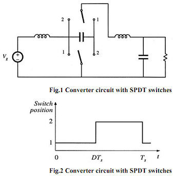
a) Realize the switches using SPST ideal switches, and explicitly define the voltage and current of each switch.

b) Express the on­state current and off­state voltage of each SPST switch in terms of the converter inductor currents, capacitor voltages, and/or input source voltage.

c) Solve the converter to determine the inductor currents and capacitor voltages.

d) Determine the polarities of the switch on­state currents and off­state voltages. Do the polarities vary with duty cycle?

e) State how each switch can be realized using transistors and/or diodes, and whether the realization requires single­quadrant, current­bidirectional two­quadrant, voltage­bidirectional two quadrant,or four­quadrant switches.

Q2. A switching converter operates with a switching frequency of 150 kHz. The converter waveforms exhibit damped sinusoidal ringing, initiated by the transistor turn­off transition, which decays slowly but eventually reaches zero before the end of the switching period. This ringing occurs in a series resonant circuit formed by parasitic inductances and capacitances in the circuit. The frequency of the ringing is 10 MHz. During the first period of sinusoidal ringing, the ac inductor current reaches a peak magnitude of 0.5 A, and the ac capacitor voltage reaches a peak magnitude of 150 V. Determine the following quantities:

(a) The value of the total parasitic inductance,

(b) The value of the total parasitic capacitance,

(c) The energy lost per switching period, associated with this ringing, and

(d) The switching loss associated with this ringing.

(e) Derive a general expression for the switching loss, as a function of the switching frequency, ringing frequency, and the ringing voltage and current peak magnitudes during the first period of ringing.

Q3. In Fig 3, the switching transition for a switch are shown with following switching characteristics:

tri = 80ns

tfv = 80ns

trv = 120ns

tfi = 200ns

Vd = 300V

I0 = 4A

217_Fig1.png

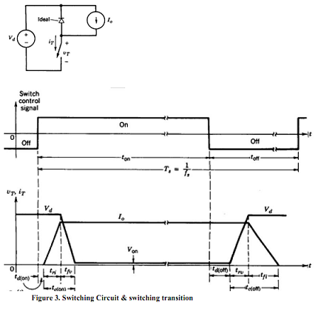
a. Using Fig 3, sketch the instantaneous switching loss for the switch as a function of time.

b. Calculate the switching power loss as a function of the switching frequency in a range 25 ­ 100 kHz, assuming Vd = 300V and I0 = 4A.

c. Calculate and plot the total losses as a function of the switching frequency in a range 25 ­ 100 kHz in the switch when the on­state voltage is Von =1.5V at 4A and the duty ratio of the switch is D = 0.4 (assume tdon=tdoff).
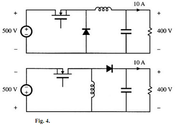
Q4. A transistor having an on­resistance of 0.5 ohm is used. To simplify the problem, you may neglect all losses other than the transistor conduction loss. You may also neglect the dependence of MOSFET on­resistance on rated blocking voltage. These simplifying assumptions reduce the differences between converters, but do not change the conclusions regarding which converter performs best in the given situations.

It is desired to interface a 500 V dc source to a 400 V, 10 A load using a dc­dc converter. Two possible approaches, using buck and buck­boost converters, are illustrated in Fig. 4, Use the assumptions described above to:

(a) Derive equivalent circuit models for both converters, which model the converter input and output ports as well as the transistor conduction loss. 

(b) Determine the duty cycles that cause the converters to operate with the specified conditions. 

(c) Compare the transistor conduction losses and efficiencies of the two approaches, and conclude which converter is better suited to the specified application.

1973_Fig2.png

Q5. To reduce the switching harmonics present in the input current of a certain buck converter, an input filter is added as shown in Figure 5. Inductors L1 and L2 contain winding resistances RL1 and RL2 respectively. The MOSFET has on­resistance Ron and the diode forward voltage drop can be modeled by a constant voltage VD plus a resistor RD. All other losses can be ignored.

1805_Fig3.png

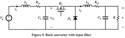
(a) Derive a complete equivalent circuit model for this circuit.

(b) Solve your model to find the dc output voltage V.

(c) Derive an expression for the efficiency. Manipulate your expression into a form similar to the below equation.

1671_Fig4.png

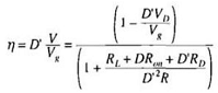
Q6. In the Cuk converter shown in Figure 6, the MOSFET has on­resistance Ron and the diode has a constant forward voltage drop VD. All other losses can be neglected.

643_Fig5.png

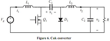
(a) Derive an equivalent circuit model for this converter. Suggestion: if you don't know how to handle some of the terms in your dc equations, then temporarily leave them as dependent sources. A more physical representation of these terms may become apparent once dc transformers are incorporated into the model.

(b) Derive analytical expressions for the converter output voltage and for the efficiency.

(c) For VD=0, plot V2/Vg vs. D over the range 0 ≤ D ≤ 1, for (i) Ron/R = 0.01, (ii) Ron/R = 0.1, (iii) Ron/R = 1. Conclude from the result. 

(d) For VD=0, plot converter efficiency vs. D over the range 0 ≤ D ≤ 1, for (i) Ron/R = 0.01, (ii) Ron/R = 0.1, (iii) Ron/R = 1. Conclude from the result.

Reference no: EM131224295

Questions Cloud

Identify default logins or user accounts for one of database : Create and document a written password policy to be given out to database users in an organization.
Describe the sourcing decision cycle framework : Describe the Sourcing Decision Cycle Framework and how it helps in making sourcing decisions. What are the key reasons for an IS organization to make its own systems? What are the key reasons for buying an application?
Describe business etiquette and customs : Briefly describe business etiquette and customs in the following areas: -  Business Greetings - Business Dress - Business Cards - Business Meetings -  Business Negotiation.
Evolution of intermodal rail freight transport : What caused the evolution of intermodal rail freight transport from its forerunning period in the 1920s to present and the future growth of the industry?
Determine the polarities of the switch on­state currents : ECE 534 Homework. Solve the converter to determine the inductor currents and capacitor voltages. Determine the polarities of the switch on­state currents and off­state voltages. Do the polarities vary with duty cycle
Inherent in the option you did not choose : Would you seek to acquire a company within the European Union or outside of it? Why? Describe the advantages and disadvantages of the choice you made. Describe the advantages and disadvantages inherent in the option you did not choose.
List the average fare permonth for each business traveler : Suppose we want to compute a data cube where the condition is that the minimumnumber of records is 10 and the average fare is over $500. Outline an efficient cubecomputation method (based on common sense about flight data distribution).
Compensation and performance appraisals : Compare the factors being measured in job-based pay, skill-based pay, and competency-based pay. - What are the advantages and disadvantages to implementing each of these measurement systems?
Government expropriated the corporations property : An American commodity broker contracted with a Cuban corporation largely owned by United States residents to buy Cuban sugar. Thereafter, subsequent to the United States Government's reduction of the Cuban sugar quota, the Cuban Government expropriat..

Reviews

Write a Review

Other Engineering Questions & Answers

  Determine discharge with recurrence interval of 100 years

Determine the discharge with a recurrence interval of 25 years - Determine the discharge with a recurrence interval of 100 years.

  Domestic wastewater treatment

Domestic Wastewater treatment using vermin-bio filtration

  Determine the optimum cross sectional area

A balanced load of 6mva is to be supplied for 2000 hours each year through a 5km three phase 11kv circuit usings kelvins law determine the optimum cross sectional area of an aluminuim conducter yo supply this load.

  Determine the average time in system

Determine the average time in system, number of passengers completing check-in, and the time-average length of the check-in queue. Put a text box in your model with the numerical results requested.

  Design latest version of that where it can show exact level

Design a latest version of that where it can show exact level of the water in over head tank by using a seven segment display.

  What is the probability that pavement will have a psi

The subgrade CBR is 8, the overall standard deviation is 0.45, the initial PSI is 4.2, and the final PSI is 2.5. What is the probability that this pavement will have a PSI above 2.5 after 25 years?

  Estimate for the standard deviation issues

If the probability of Caesarean birth is 0.30, and 140 in a sample of 500 births are Caesarean, which of these numbers is n?

  Problems baseed on a national and global perspective

How did this make you feel? If no personal situation with a supervisor, then give an example of an observation you have made.

  Determine the magnitude of resulting forces

Knowing that the drill exerts a 12 N m · couple on the piece of plywood, determine the magnitude of the resulting forces applied to the nails if the are located

  Provide table that contain each pair of voltage measurements

Provide a table that contains each pair of voltage measurements that you took (the source and diode voltages). For each pair calculate the current flowing in the circuit at that time.

  What is the output resistance rout

Replacing Q1 by its small-signal model, find an expression for the small-signal input resistance Rin assuming finite gain but infinite input  resistance for the amplifier μ. Note that here it is much easier to do the analysis directly than to use ..

  Compute secondary transformer voltage, load ripple voltage

Silicon diodes are used in a two-diode full-wave rectifier circuit to supply a load with 12 volts D.C. Assuming ideal diodes and that the load resistance is 12 ohms, compute the secondary transformer voltage, the load ripple voltage, and the effic..

Free Assignment Quote

Assured A++ Grade

Get guaranteed satisfaction & time on delivery in every assignment order you paid with us! We ensure premium quality solution document along with free turntin report!

All rights reserved! Copyrights ©2019-2020 ExpertsMind IT Educational Pvt Ltd